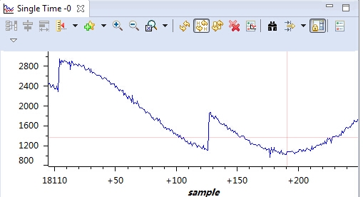
I am using TMS320F28069 to transfer ADC result0 & result 1 to the memory to do futher calculation.
Epwm3 is set to generate the triggle signal for the ADC, EPWM3 SOCA , with the code below:
   EPwm3Regs.TBPRD 				= ADC_SAMPLE_PERIOD;
   EPwm3Regs.TBCTL.bit.CTRMODE 	= TB_COUNT_DOWN;

   EPwm3Regs.ETSEL.bit.SOCASEL	= ET_CTR_ZERO;
   EPwm3Regs.ETPS.bit.SOCAPRD 	= ET_1ST;
   EPwm3Regs.ETCLR.bit.SOCA = 1;
   EPwm3Regs.ETSEL.bit.SOCAEN	= 1;
and ADC module works in the simultaneous sampling mode and transforms voltage on A1/B1, and set the answer in Result 0 & Result 1. An interupt signal (ADCINT2) will be triggered when both conversion is finished , which will trigger the DMA module.
        EALLOW;
	AdcRegs.ADCCTL1.bit.ADCREFSEL = 0;
	AdcRegs.ADCCTL1.bit.ADCBGPWD  = 1;	// Power up band gap
	AdcRegs.ADCCTL1.bit.ADCREFPWD = 1;	// Power up reference
	AdcRegs.ADCCTL1.bit.ADCPWDN   = 1;	// Power up rest of ADC
	AdcRegs.ADCCTL1.bit.ADCENABLE = 1;	// Enable ADC

	DSP28x_usDelay(1000);         // Delay before converting ADC channels

	AdcRegs.ADCCTL1.bit.INTPULSEPOS	= 1;//INT pulse generation occurs 1 cycle prior to ADC result latching into its result register
	//AdcRegs.ADCCTL2.bit.ADCNONOVERLAP = 1;	// Enable non-overlap mode
    // Select the channel to be converted when SOCx is received
	AdcRegs.ADCSOC0CTL.bit.CHSEL   = 1;
	AdcRegs.ADCSOC0CTL.bit.TRIGSEL = 9;
	AdcRegs.ADCSOC0CTL.bit.ACQPS   = 12;

	AdcRegs.INTSEL1N2.bit.INT2SEL = 1;		// IntChSel causes ADCInterrupt 2
	AdcRegs.ADCSAMPLEMODE.bit.SIMULEN0 = 1; // simultaneous sampling

	// Start-Stop conv mode
	AdcRegs.ADCINTFLG.bit.ADCINT2 = 0;  // clear interrupt flag for ADCINT2
	AdcRegs.INTSEL1N2.bit.INT2CONT = 1;	// ADCINT2 auto clr (flag clr not needed)
	AdcRegs.ADCINTSOCSEL1.all=0x0000;	// No ADCInterrupt will trigger SOCx
	AdcRegs.ADCINTSOCSEL2.all=0x0000;

	AdcRegs.INTSEL1N2.bit.INT2E = 1;		// enable ADC interrupt 2
	EDIS;

the length of the PING ro PONG is 256*16bit which lies in the DMA RAM. And we transfer 32bit per time,in which the ADC result0 lies in the low 16bit of the word and result1 lies in the high 16bit. so the source address is &(AdcResult.ADCRESULT0).  the DMA is initiated as below:
DMADest   = (Uint16*)(RFFT16_256p_in_data1);
	DMASource = (Uint16*)(&(AdcResult.ADCRESULT0));
	DMACH1AddrConfig(DMADest,DMASource);
	DMACH1BurstConfig(0,0,0);         //Will set up to use 32-bit datasize, pointers are based on 16-bit words
	DMACH1TransferConfig(256-1,0,2);      //so need to increment by 2 to grab the correct location
	DMACH1WrapConfig(0xFFFF,0,0xFFFF,0);
	DMACH1ModeConfig(DMA_SEQ2INT,PERINT_ENABLE,ONESHOT_DISABLE,CONT_ENABLE,SYNC_DISABLE,SYNC_SRC,OVRFLOW_DISABLE,THIRTYTWO_BIT,CHINT_END,CHINT_ENABLE);

	EALLOW;	// Allow access to EALLOW protected registers
	PieVectTable.DINTCH1= &DMAINTCH1_ISR;
        // Initialize PIE vector for CPU interrupt:
        PieCtrlRegs.PIEIER7.bit.INTx1 = 1;              // Enable DMA CH1 interrupt in PIE
	IER |= M_INT7 ;	                             //Enable INT7 (7.1 DMA Ch1)
	EDIS;   // Disable access to EALLOW protected registers

        StartDMACH1();

And we will change the pingpong flag in the ISR like below
interrupt void DMAINTCH1_ISR(void)     // DMA Channel 1
{

	if(FDma2Adc)
		{//buffer 2 has be filled and next destination is buffer 1
		EALLOW;
		DmaRegs.CH1.DST_BEG_ADDR_SHADOW = (Uint32)RFFT16_256p_in_data1;     // Point to beginning of Ping buffer
		DmaRegs.CH1.DST_ADDR_SHADOW = (Uint32)RFFT16_256p_in_data1;
		EDIS;
		//FDma2Adc=0;
		}
	else {
		EALLOW;
		DmaRegs.CH1.DST_BEG_ADDR_SHADOW = (Uint32)RFFT16_256p_in_data2;     // Point to beginning of Pong buffer
		DmaRegs.CH1.DST_ADDR_SHADOW = (Uint32)RFFT16_256p_in_data2;
		EDIS;
		//FDma2Adc=1;
	}
	FDma2Adc ^=1;//--- Update the Ping Pong buffer flag
	// To receive more interrupts from this PIE group, acknowledge this interrupt
	PieCtrlRegs.PIEACK.all = PIEACK_GROUP7;
	FDma2Adcready=1;

}
Thanks a lot if you has ani ideals
when i attach a 50Hz sine waveform to the A1 and the observe either of pingpong buffer it shows like below ,the sample rate is 7.042kHz. very strange isn`t it?


