This thread has been locked.

If you have a related question, please click the "Ask a related question" button in the top right corner. The newly created question will be automatically linked to this question.

Safety self test library - how to test the code?

Expert 1960 points

I have a question for SQA folks on how to test the source code on the 60730 self test library? I'm talking about both power-on-self-test (POST) and periodic self tests. Both the MCU hardware is good, everything is passed. But how do we know that when there is defect in MCU, e.g. in memory or registers, the test will fail, i.e. report the issue correctly? If we delibrately break the MCU for the sake of testing, MCU may not work at all, not even running the self test code.

Is there any software utilities to use to inject or simulate a fault? Please share your thoughts. Many thanks!

  • There are various macros set to 0 in ..\include\c28x \STL_system_config.h.

    You can set those macros to one to cause the test to fail. But this can't be done dynamically as they are predefined macros.

    the macros are named LIB_TEST_ISR_ERROR,LIB_TEST_VCU_TEST_ERROR,LIB_TEST_FPU_TEST_ERROR etc...

    Thanks

    Noah

  • Thanks Noah! I noticed some macros in the library for making the code to fail intentionally.  We'd have to build a special version for testing, and rebuild after the test. I'd prefer to have the code built and tested by independent ways, either through third party software or hardware by SQA folks.  Are there any utilities for this purpose, used by TI? Theoretically you should be able to change the registers or memory contents with CodeComposerStudio via JTAG. But it'd be hard to do manually. Is there any scripting function in CCS to do this? Just try to brainstorm for ideas.  Thanks! 

  • There is a DSS script that can be utilized to automate things you mentioned. I have attached a wiki link to get you started.

    Thanks

    Noah

  • Thanks again Noah! Further on that line: is there any example DSS scripts that is used by TI to test this library (IEC 60730), or other similar code? What we want is something special. We just want to have a way to test this code, as part of the overall software. I'd be great if we can use some help instead of re-inventing the wheel sort of thing...

  • No DSS scripting was used during validating the library. All the error macros were all set during validation and the library was built and run -issuing error status. The DSS scripting helps you to change registers without setting the error macros. However, we didn't go that route as setting the error macros was sufficient for validating the library.

    Thanks
    Noah
  • Hi Noah,

    I would like to test the code of safety library and I have problems with March Test. In order to test it, I defined in STL_system_config.h the following:

    // These Macros are embedded in the
    // safety library function
    #define LIB_TEST_MARCH_ERROR_ASC   1
    #define LIB_TEST_MARCH_ERROR_DSC   0

    Running the example of iec60730 safety library for 28335, I always get that the result of the test is correct (0xA02D) even though  I fix gTestErrorFlag = 1 in Main.c

    When I go step by step into the assembler function STL_march_test.asm, I see that it skips the ".if LIB_TEST_MARCH_ERROR_ASC".

    loop_1:                                      ;
        MOVL    ACC, *XAR4                        ; iteration1   | iteration2
        CMPL    ACC,@XAR0                       ;    +R(0);    |    +R(1)
        B        fail_ascending_march_test,NEQ ;              |    
        .if USE_MARCH13N_TEST                 ;              |    
        MOVL    *XAR4,XT                         ;              |  
        .if LIB_TEST_MARCH_ERROR_ASC          ; %%%%%% Begin Add error
        MOV     DP,#_gErrorTestFlag    
        TBIT    @_gErrorTestFlag,#0     
        B       skip_march_asc_test1,NTC;
        MOV     AH,#MARCH_ERROR_CODE
        MOV     AL,#MARCH_ERROR_CODE
        MOVL    *XAR4,ACC            

    Is it necessary to initialize something else besides LIB_TEST_MARCH_ERROR_ASC in order to run the test? It seems like the compiler has LIB_TEST_MARCH_ERROR_ASC = 0.


    Thanks!

    Maite

  • Ramon,

    The error injection for RAM is embedded within the code. You have to recompile the library for the error injection to work for RAM unlike the other tests. Basically you have to have two different versions. One that works all the time and another that doesn't work.

    Thanks

    Noah


  • Thanks Noah! It's working!

  • Hi Noah,

    now I'm trying to implement March-C test over my RAM registers. For RAM registers from 0xC000 to 0xFFFF it works fine, but when I try to test only 9 registers of my program RAM, the test fails.

        status = STL_MARCH_TEST_testRam((uint32_t *)0x008000,(uint32_t *)0x008009);

    It fails at point "check_psa_crc_start" of STL_utility.asm going to "invalid_copy_address".

    I attach below my linker file.

    I didn't add the code sections for CPU program counter register test as I don't need to implement this test, I don't know if it could be the problem.

    I re-compile the library with STL_system_config.h like this:

    #if DEVICE_TYPE_28335
    // Safe RAM locations
    #define   BOOT_RSVD_START_ADDRESS         0x0
    #define   BOOT_RSVD_END_ADDRESS             0x4F
    #define   PIE_V_START_ADDRESS                       0xD00
    #define   PIE_V_END_ADDRESS                          0xDFF
    #define   PC_TEST_1_START_ADDRESS           0xAAA8
    #define   PC_TEST_1_END_ADDRESS               0xAAAB
    // RAM memory ranges
    #define   RAMM1_END_ADDRESS                       0x7FF
    #define   RAML0_START_ADDRESS                0x8000
    #define   RAML_END_ADDRESS                   0xFFFF
    // Flash memory ranges
    #define   FLASH_START_ADDRESS                0x300000
    #define   FLASH_END_ADDRESS                  0x337FFF
    // OTP memory ranges


    Thanks!

    Maite


    MY LINKER FILE:


    MEMORY
    {
    PAGE 0 :    /* Memòria Programa */

        /*** Programa RAM ****/
        BEGIN            : origin = 0x000000        length = 0x000002    /* BEGIN is used for the "boot to SARAM" bootloader mode */
        RAM_M0            : origin = 0x000040        length = 0x0003C0
        RAML0_L2        : origin = 0x008000        length = 0x002E00
        FLASH_C            : origin = 0x328000        length = 0x002000
        FLASH_B            : origin = 0x330000        length = 0x00A000
        FLASH_A            : origin = 0x33A000        length = 0x005E80

        BOOTROM            : origin = 0x3FE000        length = 0x001FC0    /* S'ha ampliat BOOTROM */
        RESET            : origin = 0x3FFFC0        length = 0x000002

     
        CRC_TABLE          : origin = 0x33FE80        length = 0x000100     /* Table to hold 32 golden CRC values */
        CSM_RSVD        : origin = 0x33FF80        length = 0x000076    /* Posar 0x0000 si es vol CSM (clau) */
        INICI_FLASH        : origin = 0x33FFF6        length = 0x000002    /* Part de FLASHA. usada per "boot to flash" bootloader mode. */
        CLAU_PWL        : origin = 0x33FFF8        length = 0x000008    /* Part of FLASHA.    CSM password locations. */  
        ADC_CAL            : origin = 0x380080        length = 0x000009    /* ADC_cal function */                        /* 128 bits ¡ULL! no programar amb 0000 !!! */
        /*** Code Security Module Register Structures ***/


    PAGE 1 :    /* Memòria Dades i registres */

        /*** Dades RAM ***/
        RAM_M1            : origin = 0x000400        length = 0x000400
        RAML3            : origin = 0x00AE00        length = 0x001200

        /*** Dades FLASH ***/    
        FLASH_E            : origin = 0x318000        length = 0x008000    /* FLASH  MODIFICADA! */
        FLASH_D            : origin = 0x320000        length = 0x008000    /* FLASH  MODIFICADA! */

        /*** Dades DMA RAM ***/
        RAML4            : origin = 0x00C000        length = 0x01000
        RAML5            : origin = 0x00D000        length = 0x01000
        RAML6            : origin = 0x00E000        length = 0x01000
        RAML7            : origin = 0x00F000        length = 0x01000

        /*** Memòria externa ***/
        ZONE7B            : origin = 0x20FC00        length = 0x000400

        /*** Peripheral Frame 0 Register Structures ***/
        DEV_EMU            : origin = 0x000880        length = 0x000180    /* device emulation registers */
        FLASH_REGS        : origin = 0x000A80        length = 0x000060    /* FLASH registers */
        CSM                : origin = 0x000AE0        length = 0x000010    /* code security module registers */
        ADC_MIRROR        : origin = 0x000B00        length = 0x000010    /* ADC Results register mirror */
        XINTF            : origin = 0x000B20     length = 0x000020   /* External interface registers XINTF */    
        CPU_TIMER0        : origin = 0x000C00        length = 0x000008    /* CPU Timer0 registers */
        CPU_TIMER1        : origin = 0x000C08        length = 0x000008    /* CPU Timer0 registers (CPU Timer1 & Timer2 reserved TI use)*/
        CPU_TIMER2        : origin = 0x000C10        length = 0x000008    /* CPU Timer0 registers (CPU Timer1 & Timer2 reserved TI use)*/
        PIE_CTRL        : origin = 0x000CE0        length = 0x000020    /* PIE control registers */
        PIE_VECT        : origin = 0x000D00        length = 0x000100    /* PIE Vector Table */    
        DMA                : origin = 0x001000        length = 0x000200   /* DMA register */

        /*** Peripheral Frame 2 Register Structures ***/
        MCBSPA            : origin = 0x005000        length = 0x000040   /* McBSP-A register */
        MCBSPB            : origin = 0x005040        length = 0x000040   /* McBSP-B register */    
        ECANA            : origin = 0x006000        length = 0x000040    /* eCAN-A control and status registers */
        ECANA_LAM        : origin = 0x006040        length = 0x000040    /* eCAN-A local acceptance masks */
        ECANA_MOTS        : origin = 0x006080        length = 0x000040    /* eCAN-A message object time stamps */
        ECANA_MOTO        : origin = 0x0060C0        length = 0x000040    /* eCAN-A object time-out registers */
        ECANA_MBOX        : origin = 0x006100        length = 0x000100    /* eCAN-A mailboxes */
        ECANB            : origin = 0x006200        length = 0x000040    /* eCAN-B control and status registers */
        ECANB_LAM        : origin = 0x006240        length = 0x000040    /* eCAN-B local acceptance masks */
        ECANB_MOTS        : origin = 0x006280        length = 0x000040    /* eCAN-B message object time stamps */
        ECANB_MOTO        : origin = 0x0062C0        length = 0x000040    /* eCAN-B object time-out registers */
        ECANB_MBOX        : origin = 0x006300        length = 0x000100    /* eCAN-B mailboxes */

        EPWM1            : origin = 0x006800        length = 0x000022    /* Enhanced PWM 1 registers */
        EPWM2            : origin = 0x006840        length = 0x000022    /* Enhanced PWM 2 registers */
        EPWM3            : origin = 0x006880        length = 0x000022    /* Enhanced PWM 3 registers */
        EPWM4            : origin = 0x0068C0        length = 0x000022    /* Enhanced PWM 4 registers */
        EPWM5            : origin = 0x006900        length = 0x000022    /* Enhanced PWM 5 registers */
        EPWM6            : origin = 0x006940        length = 0x000022    /* Enhanced PWM 6 registers */

        ECAP1            : origin = 0x006A00        length = 0x000020    /* Enhanced Capture 1 registers */
        ECAP2            : origin = 0x006A20        length = 0x000020    /* Enhanced Capture 2 registers */
        ECAP3            : origin = 0x006A40        length = 0x000020    /* Enhanced Capture 3 registers */
        ECAP4            : origin = 0x006A60        length = 0x000020    /* Enhanced Capture 4 registers */        
        ECAP5            : origin = 0x006A80        length = 0x000020    /* Enhanced Capture 5 registers */
        ECAP6            : origin = 0x006AA0        length = 0x000020    /* Enhanced Capture 6 registers */

        EQEP1            : origin = 0x006B00        length = 0x000040    /* Enhanced QEP 1 registers */
        EQEP2            : origin = 0x006B40        length = 0x000040    /* Enhanced QEP 2 registers */    

        GPIOCTRL        : origin = 0x006F80        length = 0x000040    /* GPIO control registers */
        GPIODAT            : origin = 0x006FC0        length = 0x000020    /* GPIO data registers */
        GPIOINT            : origin = 0x006FE0        length = 0x000020    /* GPIO interrupt/LPM registers */
        /*** Peripheral Frame 2 Register Structures ***/
        SYSTEM            : origin = 0x007010        length = 0x000020    /* System control registers */
        SPIA            : origin = 0x007040        length = 0x000010    /* SPI-A registers */
        SCIA            : origin = 0x007050        length = 0x000010    /* SCI-A registers */
        XINTRUPT        : origin = 0x007070        length = 0x000010    /* external interrupt registers */

        ADC                : origin = 0x007100        length = 0x000020    /* ADC registers */

        SPIB            : origin = 0x007740        length = 0x000010    /* SPI-B registers */
        SCIB            : origin = 0x007750        length = 0x000010    /* SCI-B registers */
        ***            : origin = 0x007760        length = 0x000010    /* SPI-C registers */
        SCIC            : origin = 0x007770        length = 0x000010    /* SCI-C registers */
        SPID            : origin = 0x007780        length = 0x000010    /* SPI-D registers */
        I2CA            : origin = 0x007900        length = 0x000040    /* I2C-A registers */
        CSM_PWL            : origin = 0x33FFF8        length = 0x000008    /* Part of FLASHA.    CSM password locations. */  
        PARTID            : origin = 0x380090        length = 0x000001    /* Part ID register location */
    }
     
     
    SECTIONS
    {
        .reset                : > RESET            PAGE = 0    TYPE = DSECT

        codestart            : > INICI_FLASH        PAGE = 0

        .text                : > FLASH_B            PAGE = 0
        .cinit                : > FLASH_C            PAGE = 0
        .pinit                : > FLASH_C            PAGE = 0
        .switch                : > FLASH_C            PAGE = 0

        .const                : > FLASH_D            PAGE = 1    /*d cambio de page para ser correcto */
        .econst                :    LOAD = FLASH_D
                                RUN = RAML3
                                                LOAD_START(_econst_loadstart)
                                                LOAD_END(_econst_loadend)
                                                RUN_START(_econst_runstart)
                                                PAGE = 1    /*d cambio de page para ser correcto */

        .bss                : > RAM_M1            PAGE = 1    /*d cambio de page para ser correcto */
        //.bss                : > RAM_L0            PAGE = 1
        .ebss                : > RAML3            PAGE = 1
        .stack                : > RAM_M1            PAGE = 1
        .sysmem                : > RAM_M1            PAGE = 1    /*d cambio de page para ser correcto */
        .esysmem            : > RAM_M1            PAGE = 1

        /* ¿hacen falta? */
        .cio                : > RAM_M0            PAGE = 0
        UnderflowInt        : > RAML3            PAGE = 1

        csmpasswds          : > CLAU_PWL        PAGE = 0
        csm_rsvd            : > CSM_RSVD         PAGE = 0

        /*** Direccionament de les funcions crítiques a la RAM ***/
        ramfuncs            :    LOAD = FLASH_B
                                RUN = RAML0_L2,
                                                LOAD_START(_RamFuncs_loadstart)
                                                LOAD_END(_RamFuncs_loadend)
                                                RUN_START(_RamFuncs_runstart)
                                                PAGE = 0


         psa_crc             : LOAD = FLASH_C
                                RUN = RAML0_L2,
                                     LOAD_START(_PSA_CRCLoadStart)
                                     LOAD_END(_PSA_CRCLoadEnd)
                                     RUN_START(_PSA_CRCRunStart)
                                     RUN_END(_PSA_CRCRunEnd)
                                     LOAD_SIZE(_PSA_CRCLoadSize)
                                     PAGE = 0


        IQmath                :    LOAD = FLASH_B
                                RUN = RAML0_L2,
                                                LOAD_START(_IQmathFlash_loadstart)
                                                LOAD_END(_IQmathFlash_loadend)
                                                RUN_START(_IQmathFlash_runstart)
                                                PAGE = 0


       STL_Test_utility  : > RAM_M1, PAGE = 1
       STL_psa_crc_vars  : > RAM_M1, PAGE = 1
       STL_crc_test_data : > FLASH_B, PAGE = 0

        IQmathTables        : >    BOOTROM            PAGE = 0    type = NOLOAD

        STL_CRC_calc           : > FLASH_B            PAGE = 0
        STL_CRC_TABLE          : > CRC_TABLE        PAGE = 0

        /*** Allocate DMA-accessile RAM sections ***/
        DMARAML4            : > RAML4            PAGE = 1
        DMARAML5            : > RAML5            PAGE = 1
        DMARAML6            : > RAML6            PAGE = 1
        DMARAML7            : > RAML7            PAGE = 1

        /*** Vectors i estructures d'usuari ***/
        Vect_prova            : > RAML4            PAGE = 1
        Array_Vrms            : > RAML5            PAGE = 1
        array_P_activa        : > RAML5            PAGE = 1
        array_I_L            : > RAML5            PAGE = 1        
        array_P_L            : > RAML5            PAGE = 1    
        /*** Allocate 0x400 of XINTF Zone 7 to storing data */
        ZONE7DATA            : > ZONE7B            PAGE = 1

        /*** Allocate ADC_cal function (pre-programmed by factory ***/
        .adc_cal            : load = ADC_CAL    PAGE = 0    TYPE = NOLOAD


        /*** PIE Vector Table ***/
        PieVectTableFile    : > PIE_VECT        PAGE = 1
        /*** Peripheral Frame 0 Register Structures ***/
        DevEmuRegsFile        : > DEV_EMU            PAGE = 1
        FlashRegsFile        : > FLASH_REGS        PAGE = 1
        CsmRegsFile            : > CSM                PAGE = 1
        AdcMirrorFile        : > ADC_MIRROR        PAGE = 1    
        XintfRegsFile        : > XINTF            PAGE = 1
        CpuTimer0RegsFile    : > CPU_TIMER0        PAGE = 1
        CpuTimer1RegsFile    : > CPU_TIMER1        PAGE = 1
        CpuTimer2RegsFile    : > CPU_TIMER2        PAGE = 1    
        PieCtrlRegsFile        : > PIE_CTRL        PAGE = 1    
        DmaRegsFile            : > DMA                PAGE = 1
        
        /*** Peripheral Frame 3 Register Structures ***/
        McbspaRegsFile        : > MCBSPA            PAGE = 1
        McbspbRegsFile      : > MCBSPB            PAGE = 1
            
        /*** Peripheral Frame 1 Register Structures ***/
        ECanaRegsFile        : > ECANA            PAGE = 1
        ECanaLAMRegsFile    : > ECANA_LAM        PAGE = 1    
        ECanaMboxesFile        : > ECANA_MBOX        PAGE = 1
        ECanaMOTSRegsFile    : > ECANA_MOTS        PAGE = 1
        ECanaMOTORegsFile    : > ECANA_MOTO        PAGE = 1
        ECanbRegsFile        : > ECANB            PAGE = 1
        ECanbLAMRegsFile    : > ECANB_LAM        PAGE = 1    
        ECanbMboxesFile        : > ECANB_MBOX        PAGE = 1
        ECanbMOTSRegsFile    : > ECANB_MOTS        PAGE = 1
        ECanbMOTORegsFile    : > ECANB_MOTO        PAGE = 1
        
        EPwm1RegsFile        : > EPWM1            PAGE = 1    
        EPwm2RegsFile        : > EPWM2            PAGE = 1    
        EPwm3RegsFile        : > EPWM3            PAGE = 1    
        EPwm4RegsFile        : > EPWM4            PAGE = 1    
        EPwm5RegsFile        : > EPWM5            PAGE = 1    
        EPwm6RegsFile        : > EPWM6            PAGE = 1
        
        ECap1RegsFile        : > ECAP1            PAGE = 1    
        ECap2RegsFile        : > ECAP2            PAGE = 1    
        ECap3RegsFile        : > ECAP3            PAGE = 1    
        ECap4RegsFile        : > ECAP4            PAGE = 1
        ECap5RegsFile        : > ECAP5            PAGE = 1    
        ECap6RegsFile        : > ECAP6            PAGE = 1

        EQep1RegsFile        : > EQEP1            PAGE = 1    
        EQep2RegsFile        : > EQEP2            PAGE = 1    
                    
        GpioCtrlRegsFile    : > GPIOCTRL        PAGE = 1
        GpioDataRegsFile    : > GPIODAT            PAGE = 1
        GpioIntRegsFile        : > GPIOINT            PAGE = 1

        /*** Peripheral Frame 2 Register Structures ***/
        SysCtrlRegsFile        : > SYSTEM            PAGE = 1
        SpiaRegsFile        : > SPIA            PAGE = 1
        SciaRegsFile        : > SCIA            PAGE = 1
        XIntruptRegsFile    : > XINTRUPT        PAGE = 1
        AdcRegsFile            : > ADC                PAGE = 1
        SpibRegsFile        : > SPIB            PAGE = 1
        ScibRegsFile        : > SCIB            PAGE = 1
        SpicRegsFile        : > ***            PAGE = 1
        ScicRegsFile        : > SCIC            PAGE = 1
        SpidRegsFile        : > SPID            PAGE = 1
        I2caRegsFile        : > I2CA            PAGE = 1

        /*** Code Security Module Register Structures ***/
        CsmPwlFile            : > CSM_PWL            PAGE = 1

        /*** Device Part ID Register Structures ***/
        PartIdRegsFile        : > PARTID            PAGE = 1
    }

    /*
    //===========================================================================
    // End of file.
    //===========================================================================
    */


  • Ramon,

    Most probably you are trying to test the "check_psa_crc_start" RAM region. which is designated as safe RAM region.

    Safe RAM regions should be tested with STL_MARCH_TEST_testSafeRam() function. Please refere to Appendix C of

    the user guide for more info.

    Thanks

    Noah

  • Hi Noah,

    you are right. I already thought about this, but I wasn't able to know which region is psa_crc_code in my RAML0_L2 defined as:

    RAML0_L2  : origin = 0x008000  length = 0x002E00

    In RAML0_L2 in my linker file I have "ramfuncs", "psa_crc" and "IQmath"

    I tried to find in m .map file but it appears this:

    psa_crc    0    00008000    00000000     UNINITIALIZED

    I know that I need different March Test functions for Safe Ram and for the others, my problem is that I don't know the value of PSA_CCRunStart and PSA_CRCRunEn.


    Thanks!


  • Ramon,


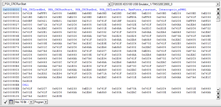
    You can find out the address from the memory debug window. Enter _PSA_CCRunStart and _PSA_CCRunStart to find out the addresses.

    Thanks

    Noah

  • Hi Noah,

    I think I have some problem with my linker file, since I have  at the same address (0x8000) all of this:

    In my .map file I have:

    GLOBAL SYMBOLS: SORTED BY Symbol Address

    page  address   name                                        
    ----  -------   ----                                        
    0     00008000  _Interrupcio_ePWM1                          
    0     00008000  _PSA_CRCLoadEnd                             
    0     00008000  _PSA_CRCLoadStart                           
    0     00008000  _PSA_CRCRunEnd                              
    0     00008000  _PSA_CRCRunStart       

    I compare with the example of IEC60730 library for F28335 with my code, and I can't find the problem with the inicialization of psa_crc.


    Did you find anything wrong in my linker file ? Specially with ramfuncs and psa_crc sections.

    Thanks!

  • Ramon,

    0     00008000  _PSA_CRCLoadStart 

    will definitely cause a problem. Because you are passing a value of a safeRAM region. I also see you have an interrupt copied to this location.

    Can you step through the memcpy function to see if things are being over written ?  I am suspecting ramfuncs and psa_crc are overlapping.

    Also can you add a  LOAD_SIZE(_RamfuncsLoadSize) to the ramfuncs section and see if that helps ?

    Thanks

    Noah

  • Hi Noah,

    I debug with breakpoints at the different calls of memcpy functions but I can't see that RAM memory registers change. I don't know which is the best way to see this. For sure that psa_crc and ramfuncs are overlapping, since I can see that  PSA_CRCLoadSize = 0, so the linker writes psa and ramfuncs starting at 0x8000.

    I also tried to add a LOAD_SIZE to ramfuncs as you mentioned, but this doesn't help.

    I assume that PSA_CRCLoadSize = 0 since I don't assign anything to this section because for the moment, I'm not using CRC calculations. I tried to not initialize psa_crc section and not doing     memcpy(&PSA_CRCRunStart, &PSA_CRCLoadStart, (Uint32)&PSA_CRCLoadSize, but then when I compile I have the following error. (In my code, for the moment,  I'm only using STL_MARCH_TEST_testRam).


     undefined        first referenced                                                                                                                                                       
      symbol              in file                                                                                                                                                            
     ---------        ----------------                                                                                                                                                       
     _PSA_CRCRunEnd   _________________________\lib\IEC60730_F28335_STL_maite.lib<STL_march_test.obj>
     _PSA_CRCRunStart _________________________ \lib\IEC60730_F28335_STL_maite.lib<STL_march_test.obj>

    error #10234-D: unresolved symbols remain
    warning #10063-D: entry-point symbol other than "_c_int00" specified:
       "code_start"


    I'm really lost with this issue! In the F28335 iec 60730 example, where did you assign some code to "psa_crc". How can I do it in my application?


    Thank you!


  • Hi Ramon,

    I am not sure why you are getting the above errors. The best thing would be to start working from the examples and change things gradually.

    None of the three functions that are copied into RAM in main.c should overlap.

    the psa_crc code routine is assigned to the memory location in STL_crc_test.asm file.

    Thanks

    Noah

  • Hi Noah,
    I solved the overlapping of "ramfuncs" and "psa_crc" introducing the function STL_CRC_TEST_testRam in my code, unless I don't need this, so I do:

    if(var_aux2 == 1)
    {
    STL_CRC_TEST_testRam((uint32_t *)start_address_march_RAM_partial,(uint32_t *)end_address_march_RAM_partial,(uint64_t *)&status);
    }
    and var_aux2 = 0 always. Doing this, I get PSA_CRCRunStart and PSA_CRCRunEnd in a different position than ramfuncs. The problem was that I initialize psa_crc section but I didn't have code associated with this, so its length was 0 and the linker overlaped it wih ramfuncs.

    Now, I have 2 problems.

    1. When I finish to load program in flash, i get the "Initialized RAM Data Warning". I checked my .map file and I think that it is due to, because if I comment STL_CRC_TEST_testRam( ) in my code I don't get this warning.

    STL_psa_crc_vars
    * 1 0000051a 00000002
    0000051a 00000002 IEC60730_F28335_STL_maite.lib : STL_crc_test.obj (STL_psa_crc_vars)

    Because this section is initialized and in my .cmd file I did the same as in the example (define the RAM but not the FLASH from where it loads):

    STL_psa_crc_vars : > RAM_M1, PAGE = 1


    I'm using CCS 3.3 and I've read in other posts: In CCS 3.3 - the flash tools would give this warning even if a section loaded to flash but ran from RAM. In this case if the .map file has been verified you can ignore this message.

    I'm not sure If I'm doing some mistake.


    2. I do the March Test of Program RAM inside an interruption that is the most priority one. I ensure by controlling the timing that I always have enouth time to test 8 registers of RAM. So I split the RAM memory test in steps of 8 registers.

    This works perfect with data RAM and for some registers of program RAM.
    However, when I reach some registers af program RAM I have and ILLEGAL_ISR trap. This interruption from where I run the March Test, is run from "ramfuncs", which it is in this RAM that I'm testing, I think that this is the problem, but I thought that by copying the RAM and restoring it back it should be fine. Which is the best way to test Program RAM not affecting the program execution?

    Thank you very much!
  • Ramon,

    1. The safety library was developed and tested with CCSv5.0 and later versions. Unfortunately there is no support for older vversions of CCS. The issue you encountered could be because of older compiler/linker issues.I suggest you upgrade to CCSv5 or later.
    2. Testing of RAM inside an ISR is not recommended. In fact the user guide suggests disabling of all interrupts before calling any safety fuctions. One issue that might arrise is what you are experienceing. You are testing RAM program section which holds an ISR for other interrupt vectors. So when an interrupt happens it is executing either an illegal opcode. I suggest you take out the RAM test from interrupt and also disable any interrupt before invoking any test function. You can find an idle time witthin your application and call the safety functions in that idle slot.

    Thanks

    Noah


  • Hi Noah,

    thanks for the answer.  In the F28335 safety library example, how is assigned that psa_crc run address in RAM is at the beginning, before ramfuncs.I couldn't find any initialization of PSA_CRCRunStart.

    I would like to do something similar in my application in order to have PSA_CRCRunStart and PSA_CRCRunEnd at the beginning of RAM_L0 (0x8000) and then have the rest of program code.

    Thanks!!

    maite

  • Ramon,
    You can easily do that. Please look at how the pc_test_section_1 is assigned to a specific location. You can follow the same approach to assign psa_crc to
    you choice of memory location.ThanksNoah
  • Hi Noah,

    thanks for the answer, now I have psa_crc section where I want.

    One question about March Test on SafeRam. The only difference with " STL_MARCH_TEST_testRam"  and "STL_MARCH_TEST_testSafeRam" is that the user doesn't have to copy and restore the contents of safe RAM?

    Is it possible to use "STL_MARCH_TEST_testRam" for testing stack section (Safe Ram) if I coment this 3 lines in "STL_march_test.asm"?

    ;  FFC     XAR7,STL_UTILITY_assertSafeRamAddress ; Assert we are not accessing safe RAM areas
    ;  CMPB    AL, #TEST_FAILED
    ;  B       end_march_RAM_test,EQ                                       ; Exit if error on memory address

    I would like to split the test in different parts and using STL_MARCH_TEST_testRam I can define the start and end addresses. I would copy the contents of stack and restore them back after the test.

    Thank you!

    Maite

  • Ramon,

    you are correct about the differences. And you can comment out the code sections and use the testRam to test stack.

    Thanks

    Noah

  • Hi Noah,

    now I'm implementing FPU Registers Test. It works fine, the problem is when I want to test the function with LIB_TEST_FPU_TEST_ERROR.

    I compiled the library with the following macros:

    #define LIB_TEST_VCU_TEST_ERROR    1

    #define LIB_TEST_FPU_TEST_ERROR    1
    #define LIB_TEST_CPU_TEST_ERROR    1

    but the only one that works is the error introduction in CPU registers test.

     .if LIB_TEST_CPU_TEST_ERROR
     .ref    _gErrorTestFlag
     .endif

    I took a look at STL_cpu_test.asm and I see that the only whan linked with gErrorTestFlag is CPU test.

    How is supposed to be tested the  FPU and VCU registers test functions?     .

    IB_TEST_VCU_TEST_ERROR is visible at STL_cpu_test.asm although it takes no effect when gErrorTestFlag = 1, but I can't find where LIB_TEST_FPU_TEST_ERROR  is used.

    Thank you very much

    Maite

  • Ramon,

    You can replace the LIB_TEST_VCU_TEST_ERROR that is found in the _STL_CPU_TEST_testFpuRegisters routine with LIB_TEST_FPU_TEST_ERROR or you can leave the LIB_TEST_VCU_TEST_ERROR in _STL_CPU_TEST_testFpuRegisters routine, set LIB_TEST_VCU_TEST_ERROR to 1 and test both FPU and VCU for fail execution. I will update the correct define inside _STL_CPU_TEST_testFpuRegisters on the next release.

    Thanks


    Noah


  • Hi Noah,

    I would like to read a little more about PSA CRC module, where can I find more information? The only bibliography I've found is en the documetnacion of IEC 60730 Library, but I couldn't find something in other data sheet of TMS320F28835 or technical reference.
    Thank you!

    Maite

  • Ramon,

    Unfortunately there is no other information regarding PSA besides what's in the safety library user's guide.

    Thanks

    Noah

  • Hi Noah,
    ok. I'm trying to understand how is implemented CRC test on Invariable Memory with F28335 library example. I've built the project and run it over TMS320F28835. I see that at least TEST_FLASH_SECTOR_H and TEST_FLASH_SECTOR_G return status = 0. I stepped into the .asm function and I can see that the value calculated by the PSA is 0 (addresses 0x0842 and 0x0843). I followed this flush_pipeline function and I see through Memory brower that registers from 0x0840 to 0x0846 are not modified.

    Can you explain me how can I follow this flash CRC tests with the example, please?

    Thankyou


    flush_pipeline:
    MOVW DP,#clearDataBus
    MOVL ACC,@clearDataBus ; Clear the data bus to a known value of 0
    EALLOW
    MOVL XAR0,#PSA_BASE_ADDRESS ; Point to the PSA base register
    MOV *+XAR0[6],#CLAIM_PSA_DRDB ; Claim Data Read Data BUS
    NOP
    NOP
    MOVL XAR0,#PSA_BASE_ADDRESS ; Point to the PSA base register
    MOV *+XAR0[6],#ENABLE_PSA_DRDB ; Enable PSA (monitor DRDB)
    EDIS
    NOP
    NOP ; NOPs for the previous operation to settle
    RPT @PH
    || ADDL ACC, *XAR4++ ; Read from memory location
    EALLOW
    MOV *+XAR0[6],#DISABLE_PSA_DRDB ; STOP PSA from caculating CRC
    EDIS
    NOP
    NOP
    end_Calculate_PSA_CRC:


    Memory brower: Data 0x840 (16-Bit Hex TI style):

    0x00000840 0000 0000 0000 0000 0000 0000 0000 0000 0000 0000
    0x0000084A 8EF0 0030 0000 0000 0422 9002 0000 0000 0000 0000
    0x00000854 0000 0000 0000 0000 0000 0000 0000 0000 0000 0000
  • Ramon,

    Please read the sections 4 and Appendix D.1.2 of the user guide carefully. Also pay close attention to the linker command file for the various PSA sections listed. The example project that shipped along with the two sectioned mentioned explain how the PSA should be used. 

    You can't use break point to step through a PSA code and get a golden CRC. If you do ,you will have different results as the PSA is cycle dependent. That's why Appendix D, details on steps to get the CRC values.

    Thanks

    Noah 

  • Hi Noah,

    sorry because I didn't read appendix D.1.2 about breakpoints on PSA CRC calculations.Now, on TI example, I can see the results in the watch window (gStrucCrcResult). Thanks.

    I tried to implement it in my application (working with CCS3.3 since it's a project started 2 years ago and almost in a release product version). About section 4, I think I've considered all the points, but something is going wrong. When I execute STL_generateCrc in Main.c I get all 0 in gStructCrcResult (without breakpoints). I have disabled the interrupts and also the flash pre-fetch. I run this function from FLASH_G, where I don't calculate CRC.

    I'm not sure that I'm linking correctly PSA calculations correctly. I attach my linker file, please, if you could take a look on it I would really appreciate. Specially on PSA CRC sections. 

    For me it's resulting very difficult to understand and follow the code of PSA CRC calculations without more information about this module.

    In Main, I copied to RAM the following functions:

    	memcpy(&PSA_CRCRunStart, &PSA_CRCLoadStart, (Uint32)&PSA_CRCLoadSize);
    	memcpy(&PC_Test1RunStart, &PC_Test1LoadStart, (Uint32)&PC_Test1LoadSize);


    And I also did:


    uint16_t gErrorTestFlag = 0;
    #pragma DATA_SECTION(gErrorTestFlag,"STL_Test_utility_error")


    void STL_generateCrc(void);
    #pragma CODE_SECTION(STL_generateCrc,"STL_CRC_calc")


    STL_CRC_TEST_RESULT_Obj gStructCrcResult;
    #pragma DATA_SECTION(gStructCrcResult,"STL_Test_utility")


    void STL_TEST_REPORT_disableFlashPreFetch(void);
    #pragma CODE_SECTION(STL_TEST_REPORT_disableFlashPreFetch,"ramfuncs")


    void STL_TEST_REPORT_enableFlashPreFetch(void);
    #pragma CODE_SECTION(STL_TEST_REPORT_enableFlashPreFetch,"ramfuncs")

    Thank you very much!

    Maite

    28335_FLASH.c
    MEMORY
    {
    PAGE 0 :	/* Mem�ria Programa */
    
    	/*** Programa RAM ****/
    	BEGIN			: origin = 0x000000		length = 0x000002	/* BEGIN is used for the "boot to SARAM" bootloader mode */
    	PSA_CRC_RAM		: origin = 0x008000		length = 0x000400
    	RAML0_L21		: origin = 0x008400		length = 0x0026A8  // 8400+26A8 = 	AAA8
    	PC_TEST_1		: origin = 0x00AAA8		length = 0x000004  // AAA8 + 4  = 	AAAC
    	RAM_L22_L3		: origin = 0x00AAAC		length = 0x001554  // AAAC+1554	= 	C000
    	FLASH_G			: origin = 0x308000		length = 0x008000
    	PC_TEST_2		: origin = 0x315554 	length = 0x000004
    	FLASH_C			: origin = 0x328000		length = 0x002000
    	PC_TEST_3 		: origin = 0x32AAAC		length = 0x000004
    	FLASH_B			: origin = 0x330000		length = 0x00A000
    	FLASH_A			: origin = 0x33A000		length = 0x005E80
    
    	BOOTROM			: origin = 0x3FE000		length = 0x001FC0	/* S'ha ampliat BOOTROM */
    	RESET			: origin = 0x3FFFC0		length = 0x000002
    
     
    	CRC_TABLE  		: origin = 0x33FE80		length = 0x000100     /* Table to hold 32 golden CRC values */
    	CSM_RSVD		: origin = 0x33FF80		length = 0x000076	/* Posar 0x0000 si es vol CSM (clau) */
    	INICI_FLASH		: origin = 0x33FFF6		length = 0x000002	/* Part de FLASHA. usada per "boot to flash" bootloader mode. */
    	CLAU_PWL		: origin = 0x33FFF8		length = 0x000008	/* Part of FLASHA.	CSM password locations. */  
    	ADC_CAL			: origin = 0x380080		length = 0x000009	/* ADC_cal function */						/* 128 bits �ULL! no programar amb 0000 !!! */
    	/*** Code Security Module Register Structures ***/


    PAGE 1 :	/* Mem�ria Dades i registres */
    
    	/*** Dades RAM ***/
    	RAM_M0			: origin = 0x000050		length = 0x0003B0
    	RAM_M1			: origin = 0x000400		length = 0x000400
    
    
    	/*** Dades FLASH ***/	
    	FLASH_E			: origin = 0x318000		length = 0x008000	/* FLASH  MODIFICADA! */
    	FLASH_D			: origin = 0x320000		length = 0x008000	/* FLASH  MODIFICADA! */
    
    	/*** Dades DMA RAM ***/
    	RAML4			: origin = 0x00C000		length = 0x01000
    	RAML5			: origin = 0x00D000		length = 0x01200
    	RAML6_L71		: origin = 0x00E200		length = 0x018C0//length = 0x01DC0 //
    	RAM_L72			: origin = 0x00FAC0		length = 0x00500
    	RAM_TEST_ERROR  : origin = 0x00FFC0		length = 0x0003F
    //	RAML7			: origin = 0x00F000		length = 0x01000
    
    	/*** Mem�ria externa ***/
    	ZONE7B			: origin = 0x20FC00		length = 0x000400
    
    	/*** Peripheral Frame 0 Register Structures ***/
    	DEV_EMU			: origin = 0x000880		length = 0x000180	/* device emulation registers */
    	FLASH_REGS		: origin = 0x000A80		length = 0x000060	/* FLASH registers */
    	CSM				: origin = 0x000AE0		length = 0x000010	/* code security module registers */
    	ADC_MIRROR		: origin = 0x000B00		length = 0x000010	/* ADC Results register mirror */
    	XINTF			: origin = 0x000B20     length = 0x000020   /* External interface registers XINTF */	
    	CPU_TIMER0		: origin = 0x000C00		length = 0x000008	/* CPU Timer0 registers */
    	CPU_TIMER1		: origin = 0x000C08		length = 0x000008	/* CPU Timer0 registers (CPU Timer1 & Timer2 reserved TI use)*/
    	CPU_TIMER2		: origin = 0x000C10		length = 0x000008	/* CPU Timer0 registers (CPU Timer1 & Timer2 reserved TI use)*/
    	PIE_CTRL		: origin = 0x000CE0		length = 0x000020	/* PIE control registers */
    	PIE_VECT		: origin = 0x000D00		length = 0x000100	/* PIE Vector Table */	
    	DMA				: origin = 0x001000		length = 0x000200   /* DMA register */
    
    	/*** Peripheral Frame 2 Register Structures ***/
    	MCBSPA			: origin = 0x005000		length = 0x000040   /* McBSP-A register */
    	MCBSPB			: origin = 0x005040		length = 0x000040   /* McBSP-B register */	
    	ECANA			: origin = 0x006000		length = 0x000040	/* eCAN-A control and status registers */ 
    	ECANA_LAM		: origin = 0x006040		length = 0x000040	/* eCAN-A local acceptance masks */
    	ECANA_MOTS		: origin = 0x006080		length = 0x000040	/* eCAN-A message object time stamps */
    	ECANA_MOTO		: origin = 0x0060C0		length = 0x000040	/* eCAN-A object time-out registers */
    	ECANA_MBOX		: origin = 0x006100		length = 0x000100	/* eCAN-A mailboxes */
    	ECANB			: origin = 0x006200		length = 0x000040	/* eCAN-B control and status registers */ 
    	ECANB_LAM		: origin = 0x006240		length = 0x000040	/* eCAN-B local acceptance masks */
    	ECANB_MOTS		: origin = 0x006280		length = 0x000040	/* eCAN-B message object time stamps */
    	ECANB_MOTO		: origin = 0x0062C0		length = 0x000040	/* eCAN-B object time-out registers */
    	ECANB_MBOX		: origin = 0x006300		length = 0x000100	/* eCAN-B mailboxes */
    
    	EPWM1			: origin = 0x006800		length = 0x000022	/* Enhanced PWM 1 registers */
    	EPWM2			: origin = 0x006840		length = 0x000022	/* Enhanced PWM 2 registers */
    	EPWM3			: origin = 0x006880		length = 0x000022	/* Enhanced PWM 3 registers */
    	EPWM4			: origin = 0x0068C0		length = 0x000022	/* Enhanced PWM 4 registers */
    	EPWM5			: origin = 0x006900		length = 0x000022	/* Enhanced PWM 5 registers */
    	EPWM6			: origin = 0x006940		length = 0x000022	/* Enhanced PWM 6 registers */
    
    	ECAP1			: origin = 0x006A00		length = 0x000020	/* Enhanced Capture 1 registers */
    	ECAP2			: origin = 0x006A20		length = 0x000020	/* Enhanced Capture 2 registers */
    	ECAP3			: origin = 0x006A40		length = 0x000020	/* Enhanced Capture 3 registers */
    	ECAP4			: origin = 0x006A60		length = 0x000020	/* Enhanced Capture 4 registers */		
    	ECAP5			: origin = 0x006A80		length = 0x000020	/* Enhanced Capture 5 registers */
    	ECAP6			: origin = 0x006AA0		length = 0x000020	/* Enhanced Capture 6 registers */
    
    	EQEP1			: origin = 0x006B00		length = 0x000040	/* Enhanced QEP 1 registers */
    	EQEP2			: origin = 0x006B40		length = 0x000040	/* Enhanced QEP 2 registers */	
    
    	GPIOCTRL		: origin = 0x006F80		length = 0x000040	/* GPIO control registers */
    	GPIODAT			: origin = 0x006FC0		length = 0x000020	/* GPIO data registers */
    	GPIOINT			: origin = 0x006FE0		length = 0x000020	/* GPIO interrupt/LPM registers */
    	/*** Peripheral Frame 2 Register Structures ***/
    	SYSTEM			: origin = 0x007010		length = 0x000020	/* System control registers */
    	SPIA			: origin = 0x007040		length = 0x000010	/* SPI-A registers */
    	SCIA			: origin = 0x007050		length = 0x000010	/* SCI-A registers */
    	XINTRUPT		: origin = 0x007070		length = 0x000010	/* external interrupt registers */
    
    	ADC				: origin = 0x007100		length = 0x000020	/* ADC registers */
    
    	SPIB			: origin = 0x007740		length = 0x000010	/* SPI-B registers */
    	SCIB			: origin = 0x007750		length = 0x000010	/* SCI-B registers */
    	SPIC			: origin = 0x007760		length = 0x000010	/* SPI-C registers */
    	SCIC			: origin = 0x007770		length = 0x000010	/* SCI-C registers */
    	SPID			: origin = 0x007780		length = 0x000010	/* SPI-D registers */
    	I2CA			: origin = 0x007900		length = 0x000040	/* I2C-A registers */
    	CSM_PWL			: origin = 0x33FFF8		length = 0x000008	/* Part of FLASHA.	CSM password locations. */  
    	PARTID    		: origin = 0x380090		length = 0x000001	/* Part ID register location */
    }
     
     
    SECTIONS
    {
    	.reset				: > RESET			PAGE = 0	TYPE = DSECT 
    
    	codestart			: > INICI_FLASH		PAGE = 0
    
    	.text				: > FLASH_B			PAGE = 0
    	.cinit				: > FLASH_C			PAGE = 0
    	.pinit				: > FLASH_C			PAGE = 0
    	.switch				: > FLASH_C			PAGE = 0
    
    	.const				: > FLASH_D			PAGE = 1
    	.econst				:	LOAD = FLASH_D,
    							RUN = RAML4,
    											LOAD_START(_econst_loadstart),
    											LOAD_END(_econst_loadend),
    											RUN_START(_econst_runstart),
    											PAGE = 1	
    
    	.bss				: > RAM_M1			PAGE = 1	
    	.ebss				: > RAML5			PAGE = 1
    	.stack				: > RAM_M0			PAGE = 1
    	.sysmem				: > RAM_M1			PAGE = 1
    	.esysmem			: > RAM_M1			PAGE = 1
    
    	/* �hacen falta? */
    	.cio				: > RAM_M1			PAGE = 1
    	UnderflowInt		: > RAML4			PAGE = 1
    
    	csmpasswds      	: > CLAU_PWL		PAGE = 0
    	csm_rsvd			: > CSM_RSVD 		PAGE = 0 


    	/*** Direccionament de les funcions cr�tiques a la RAM ***/
    	ramfuncs			:	LOAD = FLASH_B,
    							RUN = RAML0_L21,
    							LOAD_START(_RamFuncs_loadstart),
    							LOAD_END(_RamFuncs_loadend),
    							RUN_START(_RamFuncs_runstart),
    							PAGE = 0
    
    
    	ramfuncs2			: 	LOAD = FLASH_B,
    							RUN = RAM_L22_L3,
    							LOAD_START(_RamFuncs2_loadstart),
    							LOAD_END(_RamFuncs2_loadend),
    							RUN_START(_RamFuncs2_runstart),
    							PAGE = 0
    	
    	psa_crc             : 	LOAD = FLASH_C,
    	 					   	RUN = PSA_CRC_RAM,
    		                 LOAD_START(_PSA_CRCLoadStart),
                             LOAD_END(_PSA_CRCLoadEnd),
                             RUN_START(_PSA_CRCRunStart),
                             RUN_END(_PSA_CRCRunEnd),
    						 LOAD_SIZE(_PSA_CRCLoadSize),
    						 PAGE = 0


    	IQmath				:	LOAD = FLASH_B,
    							RUN = RAM_L22_L3,
    							LOAD_START(_IQmathFlash_loadstart),
    							LOAD_END(_IQmathFlash_loadend),
    							RUN_START(_IQmathFlash_runstart),
    							PAGE = 0
    
    	pc_test_section_1	 : 	LOAD = FLASH_C,
    							RUN = PC_TEST_1,
    							LOAD_START(_PC_Test1LoadStart),
    							LOAD_END(_PC_Test1LoadEnd),
    							RUN_START(_PC_Test1RunStart),
    							RUN_END(_PC_Test1RunEnd),
    							LOAD_SIZE(_PC_Test1LoadSize),
    							PAGE = 0
    
    	pc_test_section_2	:	> PC_TEST_2 , 		PAGE = 0
    	pc_test_section_3 	:	> PC_TEST_3 , 		PAGE = 0
    
    	STL_Test_utility  		: > RAM_M1, 		PAGE = 1
    	STL_Test_utility_ramM1 	: > RAML4,  		PAGE = 1
    	STL_Test_utility_error  : > RAM_TEST_ERROR, PAGE = 1  // SECCI� PER LA VARIBLE gErrorTestFlag. aqusta secci� no s'analitza
    
    	STL_psa_crc_vars   		: > RAM_M1,	 		PAGE = 1
    	STL_crc_test_data 		: > FLASH_E,		PAGE = 1
    	
    	IQmathTables			: >	BOOTROM,		PAGE = 0	type = NOLOAD
    
    	STL_CRC_calc   			: > FLASH_G			PAGE = 0
    	STL_CRC_TABLE  			: > CRC_TABLE		PAGE = 0 
    
    	/*** Allocate DMA-accessile RAM sections ***/
    	DMARAML4				: > RAML4			PAGE = 1
    	DMARAML5				: > RAML5			PAGE = 1
    	DMARAML6L7				: > RAML6_L71		PAGE = 1
    //	DMARAML7				: > RAML7			PAGE = 1
    
    	/*** Vectors i estructures d'usuari ***/
    	Vect_prova				: > RAML6_L71		PAGE = 1
    	Array_Vrms				: > RAML6_L71		PAGE = 1
    	array_P_activa			: > RAML6_L71		PAGE = 1
    	array_I_L				: > RAML6_L71		PAGE = 1		
    	array_P_L				: > RAML6_L71		PAGE = 1	
    	/*** Allocate 0x400 of XINTF Zone 7 to storing data */
    	ZONE7DATA				: > ZONE7B			PAGE = 1
    
    	/*** Allocate ADC_cal function (pre-programmed by factory ***/
    	.adc_cal				: load = ADC_CAL	PAGE = 0	TYPE = NOLOAD
    
    
    	/*** PIE Vector Table ***/
    	PieVectTableFile	: > PIE_VECT		PAGE = 1
    	/*** Peripheral Frame 0 Register Structures ***/
    	DevEmuRegsFile		: > DEV_EMU			PAGE = 1
    	FlashRegsFile		: > FLASH_REGS		PAGE = 1
    	CsmRegsFile			: > CSM				PAGE = 1
    	AdcMirrorFile		: > ADC_MIRROR		PAGE = 1	
    	XintfRegsFile		: > XINTF			PAGE = 1
    	CpuTimer0RegsFile	: > CPU_TIMER0		PAGE = 1
    	CpuTimer1RegsFile	: > CPU_TIMER1		PAGE = 1
    	CpuTimer2RegsFile	: > CPU_TIMER2		PAGE = 1	
    	PieCtrlRegsFile		: > PIE_CTRL		PAGE = 1	
    	DmaRegsFile			: > DMA				PAGE = 1
    	
    	/*** Peripheral Frame 3 Register Structures ***/
    	McbspaRegsFile		: > MCBSPA			PAGE = 1
    	McbspbRegsFile      : > MCBSPB			PAGE = 1
    		
    	/*** Peripheral Frame 1 Register Structures ***/
    	ECanaRegsFile		: > ECANA			PAGE = 1
    	ECanaLAMRegsFile	: > ECANA_LAM		PAGE = 1	
    	ECanaMboxesFile		: > ECANA_MBOX		PAGE = 1
    	ECanaMOTSRegsFile	: > ECANA_MOTS		PAGE = 1
    	ECanaMOTORegsFile	: > ECANA_MOTO		PAGE = 1
    	ECanbRegsFile		: > ECANB			PAGE = 1
    	ECanbLAMRegsFile	: > ECANB_LAM		PAGE = 1	
    	ECanbMboxesFile		: > ECANB_MBOX		PAGE = 1
    	ECanbMOTSRegsFile	: > ECANB_MOTS		PAGE = 1
    	ECanbMOTORegsFile	: > ECANB_MOTO		PAGE = 1
    	
    	EPwm1RegsFile		: > EPWM1			PAGE = 1	
    	EPwm2RegsFile		: > EPWM2			PAGE = 1	
    	EPwm3RegsFile		: > EPWM3			PAGE = 1	
    	EPwm4RegsFile		: > EPWM4			PAGE = 1	
    	EPwm5RegsFile		: > EPWM5			PAGE = 1	
    	EPwm6RegsFile		: > EPWM6			PAGE = 1
    	
    	ECap1RegsFile		: > ECAP1			PAGE = 1	
    	ECap2RegsFile		: > ECAP2			PAGE = 1	
    	ECap3RegsFile		: > ECAP3			PAGE = 1	
    	ECap4RegsFile		: > ECAP4			PAGE = 1
    	ECap5RegsFile		: > ECAP5			PAGE = 1	
    	ECap6RegsFile		: > ECAP6			PAGE = 1 
    
    	EQep1RegsFile		: > EQEP1			PAGE = 1	
    	EQep2RegsFile		: > EQEP2			PAGE = 1	
    				
    	GpioCtrlRegsFile	: > GPIOCTRL		PAGE = 1
    	GpioDataRegsFile	: > GPIODAT			PAGE = 1
    	GpioIntRegsFile		: > GPIOINT			PAGE = 1
    
    	/*** Peripheral Frame 2 Register Structures ***/
    	SysCtrlRegsFile		: > SYSTEM			PAGE = 1
    	SpiaRegsFile		: > SPIA			PAGE = 1
    	SciaRegsFile		: > SCIA			PAGE = 1
    	XIntruptRegsFile	: > XINTRUPT		PAGE = 1
    	AdcRegsFile			: > ADC				PAGE = 1
    	SpibRegsFile		: > SPIB			PAGE = 1
    	ScibRegsFile		: > SCIB			PAGE = 1
    	SpicRegsFile		: > SPIC			PAGE = 1
    	ScicRegsFile		: > SCIC			PAGE = 1 
    	SpidRegsFile		: > SPID			PAGE = 1
    	I2caRegsFile		: > I2CA			PAGE = 1
    
    	/*** Code Security Module Register Structures ***/
    	CsmPwlFile			: > CSM_PWL			PAGE = 1
    
    	/*** Device Part ID Register Structures ***/
    	PartIdRegsFile		: > PARTID			PAGE = 1 
    }
    
    /*
    //===========================================================================
    // End of file.
    //===========================================================================
    */


  • Hi Noah,

    I have one question about CRC for testing invariable memory.

    I generate my Golden Values with STL_GenerateCRC function as in the example. Then, I test all the flash with STL_CRC_TEST_testNvMemory and it works fine.

    My question is about the next comment appeared in the example:

        //! - Generate CRCs. This needs to be called only once. Since Flash A is not
    	//!   monitored for CRC periodically, this function is stored and run from 
    	//!   Flash A and once application development is done, it can be commented out.
    	STL_generateCrc();

    After getting the golden values, should I comment this line? If I do, my FLASH sector where I have .text changes and I get errors in some parts of flash. I commented also in the example and I see that also section .text.2 changes (FLASHG), which is periodically analyzed.


    Why do we have to comment out this line?

    Thanks!

  • Ramon,
    This function should be #pragma-ed in a flash section that you won't be doing a CRC. It's best if you designate a Flash section to place all CRC related functions, and golden result constants. Becuase you can't do a CRC on the function that is doing a CRC.
    We use this function to generate golden CRC values since we can't calculate the CRC outside of the chip. Once you have generated the CRC, there is no need to keep this function.
    I am not so sure why you would be getting errors. I suggest you modify your linker file and dedicate a flash sector or section that will be used to store CRC related functions and data. And you won't be running any CRC check on this sector/section.
    ThanksNoah