This thread has been locked.

If you have a related question, please click the "Ask a related question" button in the top right corner. The newly created question will be automatically linked to this question.

TMDSHVMTRPFCKIT Schematic

Other Parts Discussed in Thread: TMS320F28035

I want to clarify some doubt in the TMDSHVMTRPFCKIT (TMS320F28035 Control card) schematics kit.

1) I found some DNP components in the schematics . I know DNP means “Do Not Populate” but i don’t know why the DNP components are drawn in the schematics. Is it necessary to install DNP components on board.

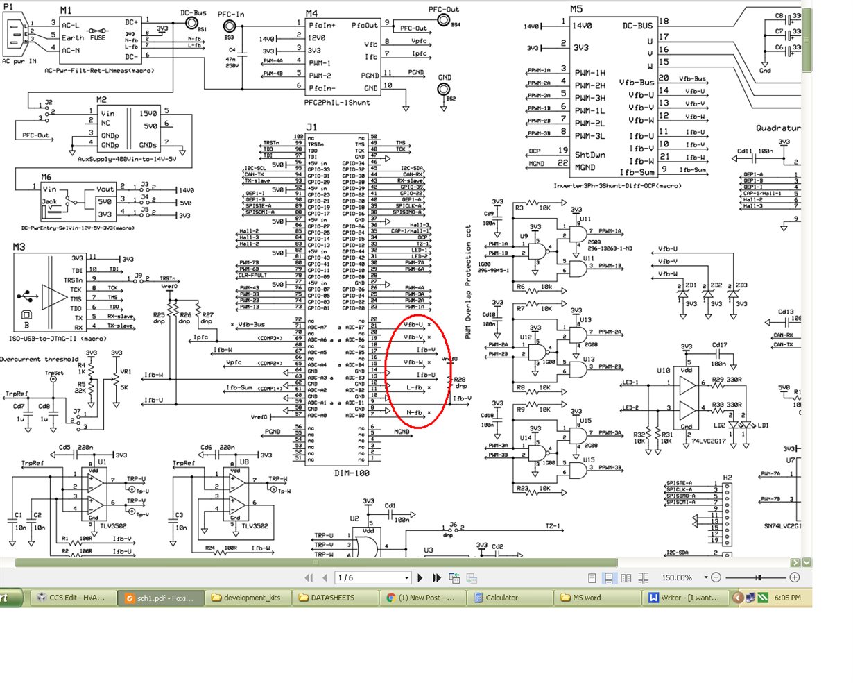
2) In schematics cross(x) is used on some feedback voltage/current pin(as shown in below image) what does it mean..? 

3)is it necessary to terminate unused ADC pin to analog ground because these pins are always defined as input pins. 

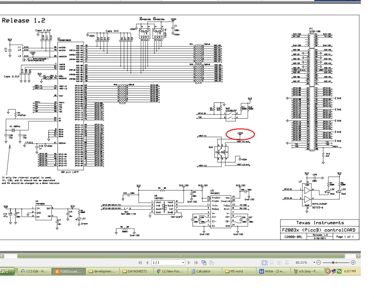
4) And last one is VDDA supply pin as shown in below image from where i can give the VDDA pin supply and how much supply..?

  • Hi Sameer,

    1) DNP (and 0ohm resistors) will occasionally be used in places where experimentation could be done.  They may also be put in places where changing the configuration of the resistor may assist in debugging.

    2) The confusing nature of how the ADCs are utilized in the design comes from several factors:

    • The hardware for the TMDSHVMTRPFCKIT and the TMDXHVMTRKIT5X are the same.  The difference between these kits is that one uses the F28055 chip (which has internal programmable gain amplifiers) whereas the other chips (F28035, F28335, etc) do not.  R25-R28 are populated on the F2805x version of the board to enable the PGA/F2805x to run the board well (Vref0 would be sourced by the F2805x chip's internal DAC).
      • The 'a' markings inside the J1 symbol represent where the F2805x controlCARD has it's PGA+ inputs.
    • There are places where an analog input is put in two or more places - the reason for this was to enable the use of the simultaneous sampling capability in many of the C2000 devices.  The F28335, F28035, F28055, F28069 all have the ability to sample ADC-A[n] and ADC-B[n] simultaneously.
    • The 'x' markings that you refer to are, to the best of my knowledge (not being the designer of the board), a mark to show that those signals do not have a constraint attached to them with respect to where they are put in the controlCARDs connector.  (it's nice to be able to put the signals that show a fault is occurring to go into comparator + inputs so that they can trip the device, the simultaneous sampling constraint as talked about above, etc)

    3) It is not necessary, but it is recommended.  Leaving ADC inputs floating gives a path for some amount of noise to enter into the chip - which may influence the ADC. 

    4) VDDA is generated based on VDDIO - you'll see where it's generated to the left of U1's pin 20.

    Hopefully this helps!


    Thank you,
    Brett