This thread has been locked.

If you have a related question, please click the "Ask a related question" button in the top right corner. The newly created question will be automatically linked to this question.

F28335 programming failure

Other Parts Discussed in Thread: TMDSDOCK28335

Hi,

I've developed a custom development board for F28335 DSC. Seems like the JTAG pin connections are correct, but it is unable to detect the target. Some things that are not correctly working are,

1. Neither the XRSn pin is toggling nor the XCLKOUT pin is not outputting anything.

2. The XRSn pin remains in HIGH and comes to LOW when RESET switch is pressed.

3. The device is not detecting at all. 

From where can I start troubleshooting? What are the possible reasons for this?

Any help would be appreciated..

Thanks,

Vishnu

  • Hi Vishnu,

    What error do you get the moment you debug?

    Regards,
    Gautam
  • thanks Gautam for the quick response...

    Now XRSn and XCLKOUt pin are working on power up. There was some soldering issue. So that got rectified. but still the device is not detecting.


    When I do test connection from target configuration window I am getting the following error.

    ===========================================
    The value is '-501' (0xfffffe0b).
    The title is 'SC_ERR_TEST_MEASURE'.
    ===========================================

    and when I do debugging using xds100v3JTAG emulator from olimex, I am getting the following error.

    =================================================
    Error connecting to the target:
    (Error -501 @ 0x0)
    The built-in scan-path length measurement failed.
    The built-in scan-path reliability tests cannot be
    performed without knowledge of the scan-path length.
    Try specifying the scan-path lengths in the command-line
    options or board configuration file of this utility or debugger.
    (Emulation package 5.1.232.0)
    =================================================


    thanks & regards,

    Vishnu
  • Hi Vishnu,

    What are XRSn and XCLKOUT doing?  Does XRSn go high after reset and does XCLKOUT toggle at around 37.5MHz (150MHz/4)?

    If you have an evaluation kit, such as the F28335 eZDSP or TMDSDOCK28335, is your xds100v3 able to connect to it?


    Thank you,
    Brett

  • Hi Brett,

    XRSn pin remains high after reset. Is it supposed to toggle ? 
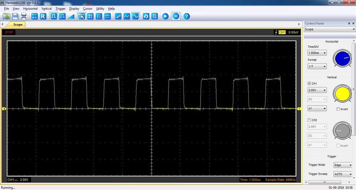
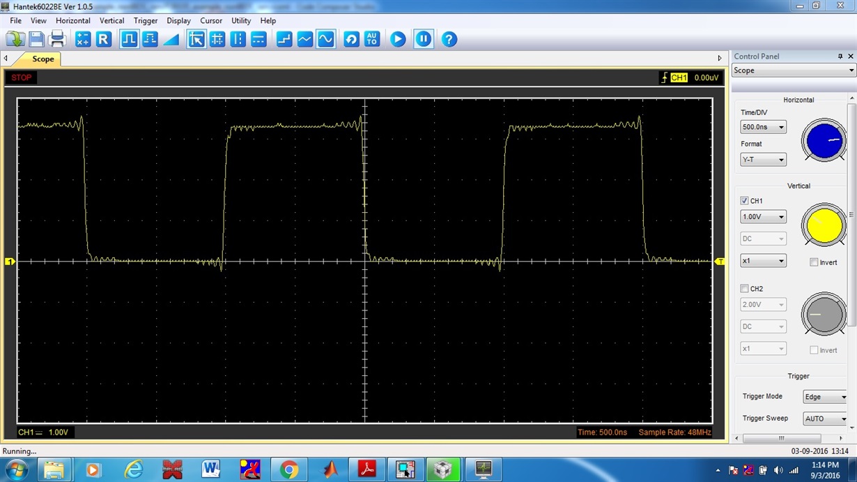
    When I press reset button(XRSn low),XCLKOUT pin toggles. The attached image shows the XCLKOUT pin when XRSn pin is low. I am using a 20MHZ crystal.

    .

    I don't have a working dev board with me right now. I could connect and debug a dev board with  xds100v2. I haven't succeeded with xds100v3 with any board til lnow since I don't have one more board. 

    thanks,

    Vishnu

  • Hi Vishnu,

    Just out of curiosity, are you and Akhil working together?
    https://e2e.ti.com/support/microcontrollers/c2000/f/171/p/538633/1966576

    The situation that you both are in is extremely similar and occurring at the same time.  If so, I'd prefer to just reply to one thread.

    In you are not working together, my comments to you are basically the same as what I just posted to Akhil's thread.


    Thank you,
    Brett

  • Brett,

    Both of us are working together. We can continue discussion here.

    The thing is XCLKOUT toggles only when RESET pin is active(held LOW). What might be the reason?  Power supply is correct as per the datasheet requirements. I am attaching JTAG pin header connection in this. Could anyone please verify if it is correct?

    In the above schematic, R53 is now replaced with 2.2K and R54 and R76 with 4.7K.  I've also attached the controller connections.

    SCHEMATIC_1_ DSP.pdf

    In this XCLKIN is now connected to ground . 

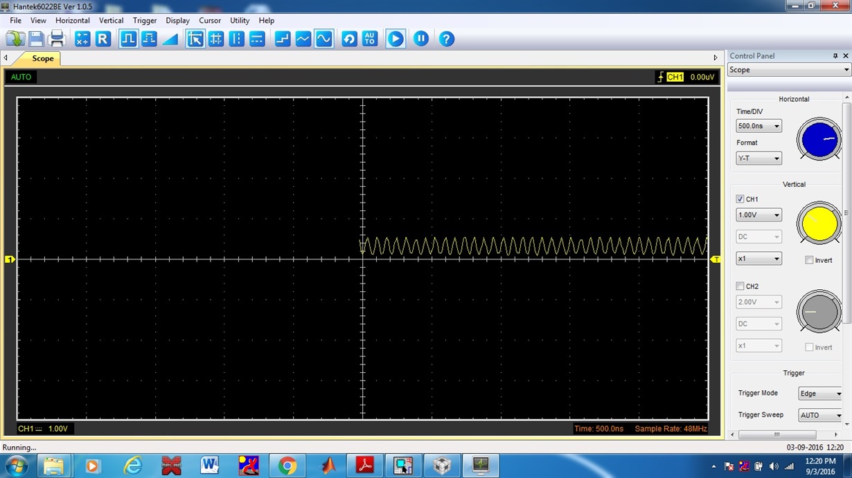
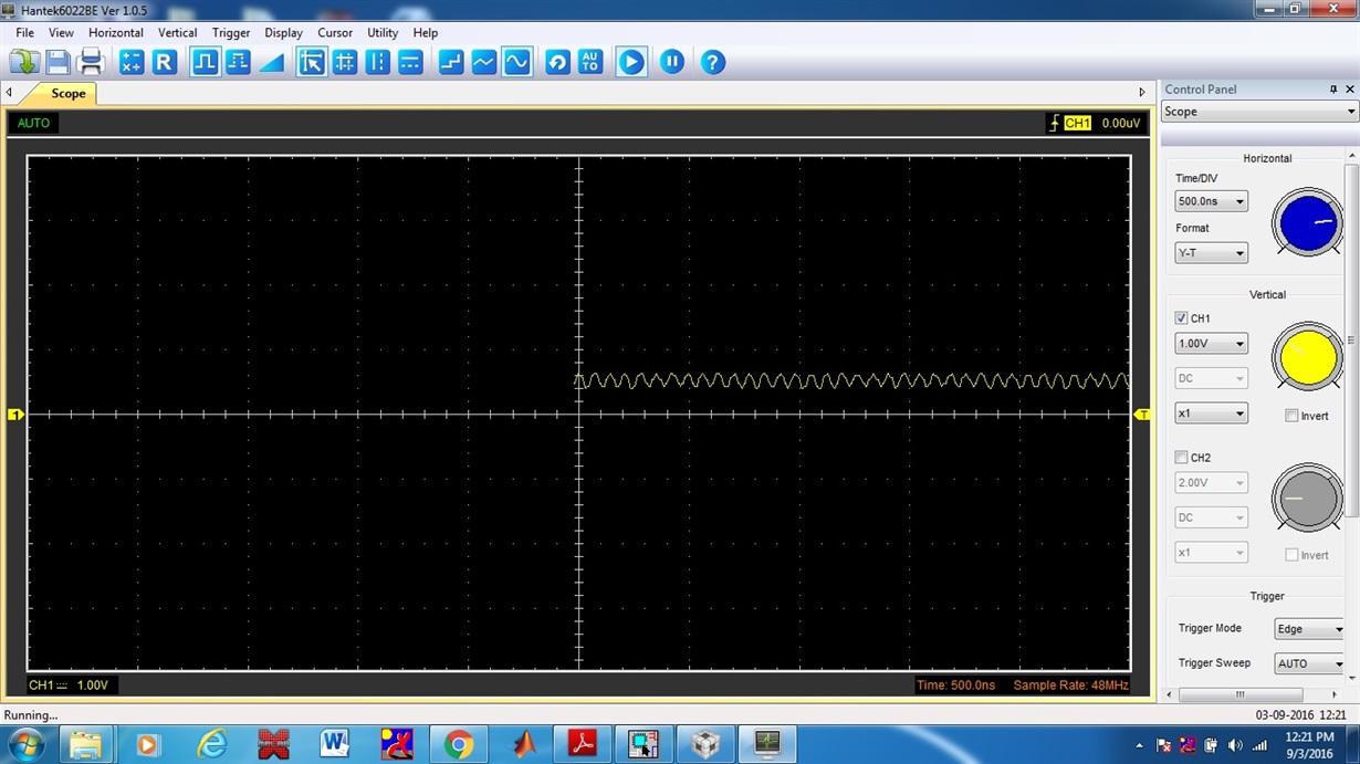
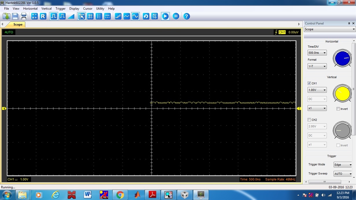
    I have also attached the scope output when probed to X1 and X2.

    This is X1 when Reset is LOW(reset button pressed)


    This is X2 when Reset is LOW(reset button pressed)

    This is X1 when Reset is HIGH(reset button is released)

    When I do debug, the TCK pin of the JTAG header gives the following, but for a short time like less than 1s. otherwise it remains LOW .

    Thanks & regards,

    Vishnu

  • Hi Vishnu,

    In your schematic, the XRSn circuitry seems to be referenced to a different set of pwr/gnd than the rest of the chip.  Looking into this would be my recommendation.

    (I would recommend having your XRSn pull-up to 3.3V be a bit stronger, ~2.2Kohm is what we commonly recommend)
    (we recommend using an external supervisor/SVS monitor the power rails of the C2000 device - at least for the 3.3V power rail)


    Thank you,
    Brett