This thread has been locked.

If you have a related question, please click the "Ask a related question" button in the top right corner. The newly created question will be automatically linked to this question.

Data logger using DSC Delfino 28335 control card with ADS804 ADC and DATA acquisition

Other Parts Discussed in Thread: ADS804, CONTROLSUITE

I also do have similar kind of requirement which is mentioned in this post http://e2e.ti.com/support/microcontrollers/c2000/f/171/t/224099,  but with higher system specification.

I'm using DSC 28335 Delfino series micro-controller and in one of the requirement i want to sample the signal at the rate of 8 to 10 MSPS with ADS804 at front end with only one channel required. Each conversion results need to be stored in memory for observation point of view that i can access later. i need data logging for the duration of 2 second.

so samples per seconds are 20MSPS of 12-bit & time is 2 Sec. so memory requirement is 640 Mbit or 40 MperWord.

Is it possible to have data logging with 28335 controller at this speed and if not i would like to invites suggestion for the same.

Thanks and Regards,

Pritesh Gohil


  • Hi Pritesh,

    A few notes:
    1) Is there a particular reason that you are using an off-chip ADC?  The internal ADC is 12bits and can do 12.5MSPS.  My assumption is that there is, but I'm just checking.
    2) With this much data AND the logging rate so fast, my feeling is that you'll need to interface your F28335 to external ASRAM via the XINTF peripheral.  Based on what I see, even with this you'll only be able to store 2M 16bit words due to the amount of address lines present.  You could potentially do something clever with GPIO to enable more address lines to be reached, but you'd have to be careful about it - and you would not have much time between writes to do too many calculations.
    3) If you keep with the ADC804, I would recommend that you make sure that the parallel data pin GPIO you choose for interfacing are part of the same bank of GPIO (ie GPADAT: GPIO00-GPIO15, or GPBDAT GPIO16-31, etc)


    Thank you,
    Brett

  • Hi Brett,

    Thankyou for your response.

    1) As per your suggestion, yes there is on chip ADC which we can use it. but it has 12.5 MSPS throughput among 8 ADC channel (i.e. SEQ1 or SEQ2). Therefore, single channel conversion rate will be 12.5/8 = 1.5625 MSPS.

    However, for the same is that possible to take sample from only one channel such that sequencer should not go to other channel for conversion as only one channel is enable. if it is possible then i'm ok with onchip ADC.

    2) In second point, it's true that we have limited address line and we can manage with GPIO. But is it good to go with extra GPIO as a address line or to choose another same series micro-controller with rich address line? if there is any which i can go, you can suggest that too.
    Also if you could give idea or perticular ASRAM it would be more helpful.

    3) Thankyou for this suggestion, this is also valuable input from you.

    thanks and Regards,
    Pritesh Gohil
  • Pritesh,

    The F28335 on-chip ADC is 12.5 MSPS.  If you setup the sequencer to convert only a single channel, then you get 12.5 MSPS on that channel.  What I would try is this.  Use the ADC in CONTINUOUS RUN mode, and setup the sequencer so that you are doing an 8 result Ping-Pong buffer.  In a nutshell: configure the clock prescalers to get the sample rate that you need (as close as you can, may not get exact).  Setup the sequencer so that all 16 channel selection registers specify the same ADC input channel (e.g. ADCINCH0).  Set MAXCONV=7 (8 conversions) and set the SEQ_OVRD bit on ADCCTRL1 register.  This will give you an interrupt every 8 conversions, and the ADC will just keep running.  In the ISR you read and process 8 ADC results, and you can manage the extra GPIO pins connected to your ASRAM so that you can page memory as needed.  What we're doing here is slowing down the interrupt rate.  Instead of getting an interrupt every ADC conversion, you get one every 8 conversions.  This gives you more time to manipulate the GPIO bits.

    Regards,

    David

  • Hi David,
    Thank you so much for the information at which i was stuck. Also the idea of getting interrupt after processing 8 ADC conversion sounds good and appreciated , the reason you mentioned we'll have enough time for the processing data and moving to the ASRAM. So conversion part can be handled with On-chip ADC instead external.

    Still one thing i can't understand, as we going to store converted data into RAM for the monitoring purpose which will be in 40 Mb(16-bit). After all converted result store let say for 2 Sec, how can we retrieve in computer to plot the graph for quick monitoring purpose?
  • Hello Pritesh,

    Pritesh Gohil said:
    Hi David,
    Still one thing i can't understand, as we going to store converted data into RAM for the monitoring purpose which will be in 40 Mb(16-bit). After all converted result store let say for 2 Sec, how can we retrieve in computer to plot the graph for quick monitoring purpose?

    You are going to have 16 to 20 Mword of data (16-bit word) in external memory (because you previously said you want to sample at 8 to 10 MSPS for 2 seconds).  This will require at least 10 manual GPIO pages of memory, since best you can get is a 2Mw page using the 21 address lines.  Yes, this will be a pain to dump to the PC.  Code Composer Studio (CCS) will let you do a memory dump, but it doesn't know anything about the GPIO paging.  You will need to manually set the GPIO, execute the memory dump, change the GPIO, dump again, and so on, until you dump all 10 pages.  You will then need to stitch these files together on the PC.  It is not as simple as just appending one file to the next since the first line of each data dump file is a header that needs to be removed (e.g. using a regular text editor).

    You could write a CCS script (or maybe a simpler GEL file) to do the 10 data dumps, and then you'd need to do something on the PC to automate the file combining.  What worries me about the GEL file is that GEL is asynchronous with the hardware.  It could start the data dump, and then change the GPIO pins before the previously started dump completes.  I'm not sure.  You'd have to test it out.

    I thought about using the SCI (UART) to transfer the data to the PC, but this does not look practical.  I calculate it will take about 47 minutes to transfer the 40 MBytes of data at 115200 baud (which is typically the fastest PC rate).

    Regards,

    David

  • Hi David,

    Thanks for your quick and valuable response. This makes my path clear to start work on the same. I will update on the same as i progress.

    Thanks and Regards,
    Pritesh Gohil
  • Hi david,

    Its good that we achieved 8.3 MSPS sample rate for our requirement. We initially decided to go with internal memory or 28335. The flow of code is like after every conversion we store our data to array . now we move this data array to FLASH from RAM.

    Is it possible during run-time writing into FLASH? How can we transfer block of data to one of the FLASH memory section?

    Thanks and Regards,
    Pritesh Gohil
  • Pritesh,

    Pritesh Gohil said:

     
    Is it possible during run-time writing into FLASH? How can we transfer block of data to one of the FLASH memory section?

    Writing to the flash is done using the flash API functions available in ControlSuite, but flash programming is very slow and I don't think it will work for you for data collection purposes.  The CPU will be consumed doing the writing during this time.  Also, while you write to the flash, you cannot access any of the other flash.  This means the active portion of your code needs to be moved to RAM.

    Regards,

    David

  • Hi David,

    Thanks for your quick response.
    I understood how difficult it will be with FLASH to manage data. But here i divided my process in 3 steps.

    1. Write code into FLASH and move ADC_ISR to RAM for quick data saving in SARAM.
    2. once data storage in SARAM completes, let say 3k word . After this to retain this data i want to transfer to the FLASH. This is not time critical operation as we have plenty time to copy 3K word into FLASH.
    3. Last stage is also not time critical, Just move data from FLASH to PC via SCI/ SPI.

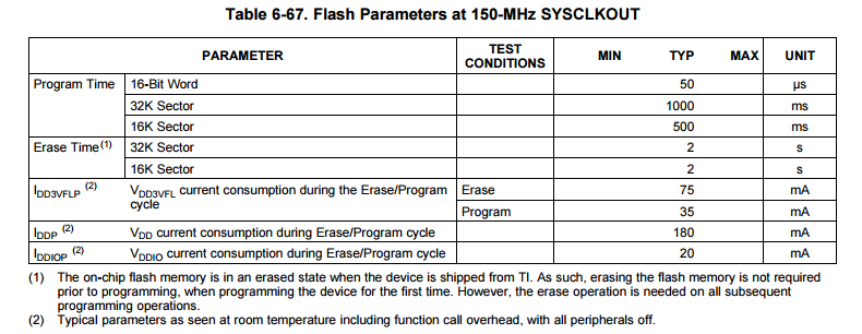
    So is 2nd and 3rd stages are possible via FLASH API ? if so How much time FLASH can take in 2nd stage to write 3k Word? could you please suggest some piece of code if available to understand how it will work?
    P.S.: timing is critical in first stage, once i have data then 2nd and 3rd stage can is not so time critical.


    Thanks and Regards,
    Pritesh Gohil
  • Hi Pritesh,

    The flash write timings can be found in the datasheet here:

    I am not sure why the flash writes won't be in the critical path if you want to sample for 2s continuously.  It only takes about 300us to fill up 3Kx16 of RAM with ADC samples, but it is going to take 100ms to program the same data into flash?  I think you will want to use an external ram with XINTF to save the data. 

    As far as getting the data to the PC, if you already have an emulator connected, you may want to look at transferring the data using "Debug Server Scripting" or DSS.  DSS is essentially a headless version of CCS you control programmatically. You could do something like repeatedly reading a 1KW array to get the data out.  I think the emulator usually gives a transfer rate of at least 1Mb/s, even with a budget emulator like XDS100 (and I believe we also make the XDS100 HW design available, so you could stamp one out on your PCB if desired).  

  • Hi Devin,

    Sorry, i forgot to mention about little deviation from initial design.
    instead going with 2 Sec, we have decided to take sample for 300-400 uS at the rate of 8.3MSPS.
    So Requirement of external Memory we postponed and going with intenal RAM.

    Awaiting for 2nd stage doubt clearance from last reply.

    Thanks and Regards,
    Pritesh Gohil