This thread has been locked.

If you have a related question, please click the "Ask a related question" button in the top right corner. The newly created question will be automatically linked to this question.

TMS320F28377S: ADC issue with first sample

Part Number: TMS320F28377S
Other Parts Discussed in Thread: REF3030, OPA2227

C2000 Team,

I am running the ADC-A on F28377S Launchpad in 12-bit mode, triggered from ePWM at 50 kHz rate, and acquisition window of 100 ns (20 cycles @ 200 MHZ SYSCLK).  I am using the CPU to take a single 50 point buffer of data.  After buffering 50 points, the ADC interrupt is disabled in the ISR so I buffer no more points.  Conversion is on ADCINA0 channel.

The problem is with the very first point.  See graphs below.  The input is a 1 kHz triangle wave running from about 0.2 to 3.1V.  The very first point is always slightly off.  You can see it in the CCS graphs below.

I added additional delay after enabling the ADCs before I trigger them with the ePWM.  No difference.

I tried a different signal generator thinking maybe it was some sort of loading issue on the input.  No difference.

I tried a different ADC (ADC-B).  No difference.

I doubled the acquisition window to 200 ns.  No difference.

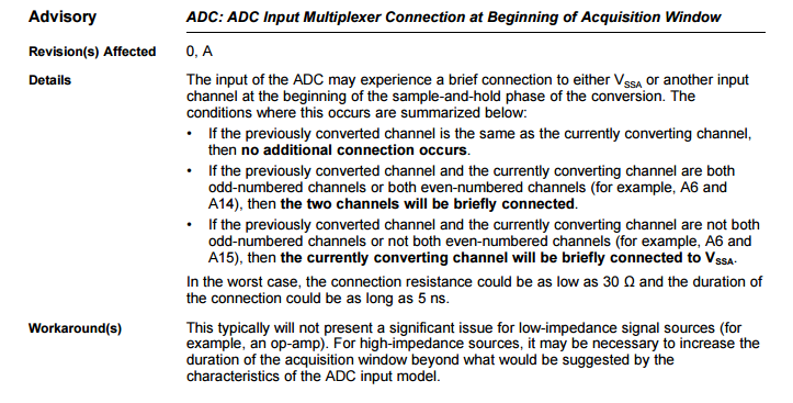
I checked the errata and don't see anything about a first sample error.

Now, I am using TMX silicon (rev.B), but this just doesn't seem like the problem.  All the other samples are fine (with some apparent offset error).

Any ideas on what could be causing this?

Thanks and regards,

David

  • Hi David,

    Some things you can try/investigate:

    The A0 channel is also mux'ed with the buffered DAC output. Even with the buffered DAC disabled there is a parasitic 50kohm load on this pin. You can try with a different ADC input to see if that helps (There is also a DAC on A1, and B1. Channel B0 is also a little bit different because it has ~100pF additional capacitance since it is a DAC reference pin).

    Not sure how much additional delay you added between ADC power-up and the first set of sampling, but 1ms should be more than enough power-up time.

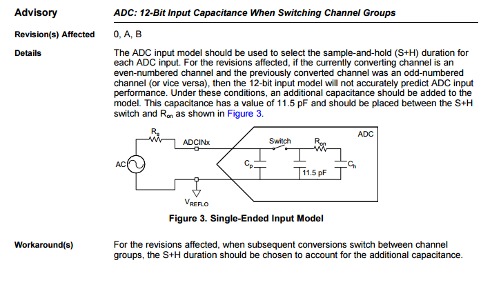
    On rev. B it requires more time for the input to settle when switching between ADC channel banks (erratum "ADC: 12-Bit Input Capacitance When Switching Channel Groups"). You could try having each trigger do A0->A1 to see if the A0 results are consistently off when always switching channel banks.

    Do you have any external capacitance or series resistance on this channel? You should be able to make the S+H really long @ ~50KHz sample rate as an easy sanity check.

    How much offset error do you see? The offset should be pretty good (<8 LSBs) even untrimmed in 12-bit mode. Some of this offset error could be due to the DAC muxing, so it would be interesting to see if this improves when using a channel other than A0.

    Are you using a ControlCard or Launchpad or a custom board? We had some issues with the ADC reference driving circuitry on earlier versions of the F28377x ControlCards.

    Is the ADC in late interrupt mode? If not, the CPU is fast enough on this device to get into the ISR and read the conversion result before it is ready.
  • Hi Devon,

    Devin Cottier said:

    Are you using a ControlCard or Launchpad or a custom board? We had some issues with the ADC reference driving circuitry on earlier versions of the F28377x ControlCards.

    I am using the F28377S Launchpad.

    Devin Cottier said:

    The A0 channel is also mux'ed with the buffered DAC output. Even with the buffered DAC disabled there is a parasitic 50kohm load on this pin. You can try with a different ADC input to see if that helps (There is also a DAC on A1, and B1. Channel B0 is also a little bit different because it has ~100pF additional capacitance since it is a DAC reference pin).

    I tried using ADCINA5.  No difference.

    Devin Cottier said:

    Is the ADC in late interrupt mode? If not, the CPU is fast enough on this device to get into the ISR and read the conversion result before it is ready.

    Yes, ADC is in late interrupt mode.

    Devin Cottier said:

    How much offset error do you see? The offset should be pretty good (<8 LSBs) even untrimmed in 12-bit mode. Some of this offset error could be due to the DAC muxing, so it would be interesting to see if this improves when using a channel other than A0.

    If I use a AA battery as the input, I can get some measure of the total error.  The battery measures 1.488 V.  Expected converted value is therefore

    x = 4096*(VIN - VREFLO)/(VREFHI - VREFLO) = 4096*(1.488 - 0)/(3.0 - 0) = 2032

    The observed value is about 0x0809 = 2057.  So, I've got combined offset and gain error totaling about 25 LSBs at mid full-scale range.  You can see the results are pretty clean below.  Interestingly, I ran this experiment several times.  The first converted value always seems a little high compared to the others.

    Below, the input is a square wave, 0V low and 2.8V high.  2.8V should convert ideally to 0xEEF.

    Again, notice that the first converted value is higher than the other "High" values. 

    Regards,

    David

  • Hi David,

    Can you measure the VREFHI pin with a DMM? How close is this to exactly 3.000V? 25 LSBs at mid-scale is quite a bit more than the expected gain and offset error (Max in the DS is +/-5LSBs for gain and +/-4LSBs for offset). Being un-trimmed/TMX shouldn't make much difference for this device. REF3030 should be within 0.2% under nominal conditions, which equates to 8 LSBs of full-scale gain error.
  • Hi Devin,

    I got a better DMM (Tektronix DMM912) out of the lab instead of the junk $10 toy meter I had at my desk.

    REF3030 output is 2.9997V (at pin 2 of U10 on F28377S Launchpad).
    VREFHIA is 2.9997V (at pin 1 of U11 on LP)
    I re-measured my AA battery: 1.5041 V

    The battery should convert to 4096*(Vin-Vreflo)/(Vrefhi - Vreflo) = 4096*(1.5041 - 0)/(2.9997 - 0) = 2054

    Actual observed converted value using ADCINA0  channel is 2065 (50 sample average. Battery connected to J3.27 on LP).
    Actual observed converted value using ADCINA12 channel is 2059 (50 sample average.  Battery connected to J3.27 on LP))
    Actual observed converted value using ADCINA5 channel is 2071 (50 sample average.  Battery connected to J7.65 on LP)

    Recall that ADCINA12 and ADCINA0 are both connected to the ADCINA0 pin on the device, so I didn't change the battery connection to the launchpad for those two measurements.  I ran the above measurements several times in various order, rebuilding the code, changing connections and running, etc.  The results seem subject to variation if you change the mechanical connection of the battery.  If you keep the connection constant, the results are mostly consistent.

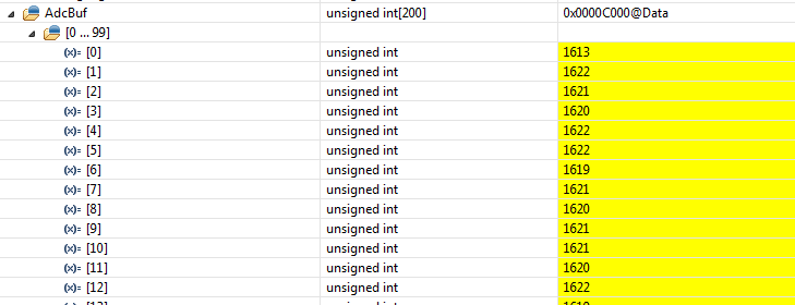
    Here are screen shots of the ADC buffer for each measurement:

    ADCINA0:

    ADCINA12:

    ADCINA5:

    I stepped through the AdcSetMode() function in my code, and it appears that the ADC offset and INL trim data are not populated on my TMX device.  Not unexpected.

    Let's forget about offset error for a moment, as I think that is under control.  If you look at the screenshots above, you see the first conversion in the buffer is much higher than the others for ADCINA0 and ADCINA5.  This does not hold for ADCINA12 for some reason.  I increased the acquisition window from 20 to 80 SYSCLK cycles, and the first value seems to fall more inline with the average.  Results are rather mixed, and seem to be jumping around a bit on me.

    - David

  • Hi David,

    I can't say that I've ever used a battery as an ADC input source.  My guess is that it doesn't have the bandwidth to properly drive an ADC input.  To use it as a DC test source, I'd recommend providing an external capacitor on the ADC pin that is at least 4096 * 4 * Ch = 4096 * 4 * 14.5pF = 238nF.  

    Better would be a function generator set to DC mode.  Adding a capacitor in the 10pF - 100pF range is usually a good practice for a proper signal source.

    You can also use a power-supply as a DC source, but you need to add some pretty significant capacitance to the output to get the noise down.  I have used a 470uF electrolytic capacitor in parallel with a 1nF ceramic capacitor and that seems to do a pretty good job.  

  • Devin,

    I added 300 nF of capacitance and it seems to help with the first sample and also offset (accuracy) of conversion with small acquisition windows.  When I cut the acquisition window down to 15 SYSCLK cycles (75 ns), I was getting a decent amount of error.  With the capacitance, the extra error seemed to go away.

    I will leave this alone at this point and move on.  One question though: Is the design such that the hold capacitor is discharged between each conversion, or does it hold its value (and perhaps slowly leak discharge)?  I think the answer is the the later (holds its value), which makes it hard to understand why a small acquisition window would give me errors once the hold cap charged up.

    Thank you,

    David

  • Hi David,

    On this device the sampling capacitor is completely discharged whenever switching between even and odd channels. When sampling the same channel bank consecutively the charge may or may not be the very close to the previous sample, depending on the SAR conversion sequence.

    Best practice is to always assume the hold capacitor could be any voltage in the reference range of the device. Usually the easiest way to model this is to assume that you are trying to drive a full-scale voltage and the capacitor starts fully discharged.
  • Hi all,

    I noticed the same problem and wanted to open a new post, but David has done before me ;)

    The problem occurs only for fist sample and at different sampling frequencies (2,5kHz, 50kHz, 100kHz respectively).

    The signal is a square wave 0 - 2v (60Hz, 1kHz, 5kHz respectively)

    The value 406! is very big mistake..

    Paolo

  • Hi Paolo,

    Same questions as for David:

    -What does your signal source look like?
    -What HW/Kit are you running this on?
  • Hy Davin, hi all

    The signal looks like to a square wave when i plot it except first sample. The Others values are generally correct even if i think that there is some lost samples.

    I haven't professional signal generator, so i use NI-Mydaq to generate the signal, but i don't think that is the problem. If so, some other samples should be wrong.


    It could be the ePWM SOC system the problem?

    Paolo.
  • Hi Paolo,

    If the signal range is 0 to 2V and you are somehow getting a calculated result > 400V I don't think the issue is purely with a bad sample...there must be a SW issue too in calculating the result because the ADC will saturate at a digital output of 4095 LSBs (with 3.0V range, 2V = 2730 LSBs).  

    It might be easier to debug if you look directly at the raw ADC output.

    What kit/HW are you using? Is this a ControlCard, launchpad, or custom board?

  • Hi Davin,

    yes i agree, i think the problem is SW.

    The variability of the value of the first element is very random: if i try to run program in debug, the numbers are different, but sometimes are right.

    I'm using C2000 Delfino MCUs F28377S LaunchPad Development Kit.

    When i go at home i try to debug directly ADC buffer and will more precise.

    Thank you very much.

    Paolo.

  • Devin,

    I've been playing around with this more today, and I'm not convinced this is a capacitance problem.  Today, I am running all four ADCs at 3.125 MSPS each, with the results interleaved.  So, effective sampling is 12.5 MSPS.  ADC Triggering is in this order: A->C->B->D.  The input is a ~1 MHz triangle wave.  Hence, there should be 12.5 samples per period.  I get about 11, which I am currently ignoring and attributing to an uncalibrated internal oscillator in the TMX silicon.  Here is a plot of the results:

    You'll notice the first sample (which comes from ADC-A) is much too high.  If you look closely, you'll see that samples 2, 3, and 4 (coming from ADC-C, B, and D respectively) are also out of alignment.  After that, the samples look good.

    I might be able to convince myself that samples 2, 3, 4 errors are due to capacitance and acquisition time, but not sample 1.  If sample 1 didn't have enough time to charge the hold capacitor, why would the converted value be too high?

    Note that I am not switching channels on any of the ADCs.  I am always converting ADCINx12, which is connected to the ADCINA0 pin for all four ADCs.

    This data was taken on an F28377D Experimenter's kit with TMX rev.B silicon.

    Regards,

    David

  • Hi David,

    Agreed; something is definitely fundamentally wrong with the first sample (and the next three are maybe a little off).

    This could be an issue with the SW timing of the first set of samples.  I am pretty confident you can effectively debug this, but some quick thoughts:

    -Ensure that you enable TBCLKSYNC after both the ADC and ePWM are fully configured and ready to sample

    -I think you have 2 ePWMs synchronized with a period of 128 and each ePWM triggers 2 ADCs?

    -ACQPS should be between  32 and 14?

    As far as HW: Which ControlCARD revision do you have plugged into the experimenter's kit?  Some older ControlCards have the wrong op-amp driving the ADC reference pins, which can be unstable and lead to some strange ADC behavior.  You can fix this by either bypassing the reference driving op-amp with a wire, or by replacing it with the correct op-amp.  On some newer ControlCard revisions, the 100m ohm resistor in series with the ADC reference capacitors has been erroneously built with a 100M ohm resistor, which can again cause some strange ADC behavior (this can be fixed by replacing the resistors with a 0-ohm or solder bridge).  

    I'd probably recommend using an external XTAL vs. the internal oscillator for high-speed signal sampling...the additional jitter is going to significantly affect the SNR @ 1MHz (note that the ADC SNR is specified at 100KHz in 12-bit mode with an external XTAL).  I think all the ControlCards have an external XTAL or clock source.  

    I'd also be interested if you stop the sampling process and then restart it if you still see an issue with the first sample?  If yes, try decreasing the time between start and stop...if the magnitude of the error scales with the time between start/stop then it would point to an analog issue, but if it is always the same even if you only stop for a couple cycles it would point to a SW issue.  

  • Devin,

    >> Ensure that you enable TBCLKSYNC after both the ADC and ePWM are fully configured and ready to sample

    Yes.

    >> ACQPS should be between  32 and 14?

    Yes.

    >> I'd also be interested if you stop the sampling process and then restart it if you still see an issue with the first sample?

    I had run this experiment more or less.  I re-ran.  I reverted back to simple code using only ADC-A triggered from an ePWM (running on F28377S Launchpad with rev.B TMX silicon).  Sample rate is 1 MHz.  Input is 8300 Hz triangle wave.  The CPU is collecting the ADC results based on SOC0 EOC interrupt.

    First thing is, that if you read the ADCARESULT0 register after reset but before completing a conversion, you read zero.  I tested this by reading the result register right after configuring the ADC (but before triggering via ePWM).  This is consistent with the TRM SPRUHX5D p.1322 showing that this register defaults to zero.

    Now, my baseline code shows the first sample issue.  You can see the error in sample #1:

    I then modified my code so that during config, I software trigger the ADC SOC0.

        AdcaRegs.ADCINTSEL1N2.bit.INT1CONT = 1;     // Interrupt pulses regardless of flag state
        AdcaRegs.ADCINTSEL1N2.bit.INT1SEL = 0;      // EOC0 triggers the interrupt
        AdcaRegs.ADCINTSEL1N2.bit.INT1E = 0;        // Disable the interrupt in the ADC
        AdcaRegs.ADCCTL1.bit.ADCPWDNZ = 1;          // Power up the ADC
        DelayUs(1000);                              // Wait 1 ms after power-up before using the ADC
        AdcaRegs.ADCSOCFRC1.bit.SOC0 = 1;           // SW trigger SOC0
        DelayUs(1000);                              // Wait long enough for end of conversion

        AdcaRegs.ADCINTSEL1N2.bit.INT1E = 1;        // Enable the interrupt in the ADC
        PieCtrlRegs.PIEIER1.bit.INTx1 = 1;          // Enable ADCA1 interrupt in PIE group 1
        IER |= 0x0001;                              // Enable INT1 in IER to enable PIE group

    I then proceed to configure the ePWM as before for triggering.  The problem goes away:

    - David

  • David,

    Can you try this: 

    AdcaRegs.ADCINTSEL1N2.bit.INT1CONT = 1; // Interrupt pulses regardless of flag state
    AdcaRegs.ADCINTSEL1N2.bit.INT1SEL = 0; // EOC0 triggers the interrupt
    AdcaRegs.ADCINTSEL1N2.bit.INT1E = 0; // Disable the interrupt in the ADC
    AdcaRegs.ADCCTL1.bit.ADCPWDNZ = 1; // Power up the ADC
    DelayUs(1000); // Wait 1 ms after power-up before using the ADC
    AdcaRegs.ADCSOCFRC1.bit.SOC0 = 1; // SW trigger SOC0
    AdcaRegs.ADCSOCFRC1.bit.SOC1 = 1; // SW trigger SOC1
    DelayUs(1000); // Wait long enough for end of conversion

    AdcaRegs.ADCINTSEL1N2.bit.INT1E = 1; // Enable the interrupt in the ADC
    PieCtrlRegs.PIEIER1.bit.INTx1 = 1; // Enable ADCA1 interrupt in PIE group 1
    IER |= 0x0001;

    Where SOC1 is configured for a channel that is even if SOC0 is configured for an odd channel or odd if SOC0 is configured for an even channel?

    Alternately, you could configure SOC0 to use the other channel bank, and then switch the channel config after the software force.

    What happens when you trigger two conversions with each ePWM event, where the second conversion is some other channel?

    Have you tried using ADCIN14/15 instead of input 12?  These inputs also fan-out to all channels, but don't experience the parasitic DAC load.  

  • Hmmm.  I configured SOC1 to convert ch.1 (odd channel).  I SW triggered SOC1 after the SW trigger of SOC0 (channel 12).  The problem with the first sample re-appeared.

    So what does this mean?  It is sounding like the first conversion in a channel bank after switching channel banks is subject to conversion errors.

    - David

  • There are two errata that cover this.  One applies to only revisions 0 and A, the other applies to 0, A, and B.  (Production TMS silicon should all be rev. C).  

    Can you confirm which errata apply to your kit(s)?

  • Devin,

    I have rev.B silicon, so the second of the two errata you show apply.  I had reviewed the errata but didn't expect this problem since I wasn't switching channels.  Apparently the first conversion for the ADC counts as a bank switch.

    I'm not completely comfortable through that this is the only source of the problem.  Even if I increase the acquisition time from 75 ns to 375 ns, I can still seem some first sample error (although not as pronounced as before).  Also, the error is often that the first sample value is too high, which I wouldn't expect from a capacitance problem.

    It seems that what I need to do is try with rev.C silicon, which I do not have unfortunately.  Both my boards use rev.B silicon.

    I will try to move on at this point.  Thank you for your help.

    - David

  • hello guys,

    i did some tests, the results seems good.

    Simply i replaced float32 input buffer with uint16_t RFFTin1Buff [DIM].

    The setting of PWM and ADC  are the same of adc_soc_epwm example. The problem seems go away, but more experiments need.

    As example a 5kHz sine wave, Fsampling = 100kHz, 2Vpp, 1.1V average

    I will do more tests and keep you informed.

    Regards,

    Paolo.

  • Hi Paolo,

    The sine wave definitely looks good.

    If the fundamental issue is turning the unsigned ADC results into an appropriately scaled floating-point value, you may want to start a new thread on that topic. You may also be able to find some help with that topic by searching other posts on e2e.

    If you end up with problems with the sampling process itself, then this thread is still probably a good place to post.
  • Hy guys, other tests i did.

    Saw tooth, 2Vpp.

    Seems all ok, no more trouble even if not always the sampling is impeccable, but good. I think the problem is type of buffer, it doesn't like float :D:D

    As soon as i want ivestigate better and eventually open a new thread on this argument.

    Best regards

    Paolo

  • Devin,

    David M. Alter said:

    I have rev.B silicon, so the second of the two errata you show apply.  I had reviewed the errata but didn't expect this problem since I wasn't switching channels.  Apparently the first conversion for the ADC counts as a bank switch.

    I'm not completely comfortable through that this is the only source of the problem.  Even if I increase the acquisition time from 75 ns to 375 ns, I can still seem some first sample error (although not as pronounced as before).  Also, the error is often that the first sample value is too high, which I wouldn't expect from a capacitance problem.

    It seems that what I need to do is try with rev.C silicon, which I do not have unfortunately.  Both my boards use rev.B silicon.

    I've been able to test this on a board with F28377D rev.C silicon.  The first sample is always off by more than the other samples.  Not by much, but it is detectable.  Here are results for a constant 2.500 V input, 3.315 V reference (both measured), 12-bit mode, ADC-A ch.12 (connected to ADCINA0) using socketed FAE board, acquisition window of 35 SYSCLK cycles (175 ns), sample rate of 50 kHz.

    The correct result should be 4096*(2.500/3.315) = 3089.  You can see that the first result has more error than any of the others.  I ran the experiment multiple times, and always get the same results.  First sample shows more error.  The problem here is far less than I was seeing with rev.B silicon.  But, it is still detectable.  Just documenting what happened here.

    Regards,

    David

  • We all look forward to a solution :)

    Regards
    Paolo
  • The problems continue...

    The behaviour is very strange, now not only first sample, but others.

    Futhermore another strange error does occurs:

    I don't know if is related to main problem.

    However i want share my program so if you want analize it to understand better the problem.

    ########################################################################
    // FILE:   adc_soc_epwm_cpu01.c
    // TITLE:  ADC triggering via epwm for F2837xS.
    //
    //! \addtogroup cpu01_example_list
    //! <h1> ADC ePWM Triggering (adc_soc_epwm)</h1>
    //!
    //! This example sets up the ePWM to periodically trigger the ADC.
    //!
    //! After the program runs, the memory will contain:\n
    //! - \b AdcaResults \b: A sequence of analog-to-digital conversion samples from
    //! pin A0. The time between samples is determined based on the period
    //! of the ePWM timer.
    //
    //###########################################################################
    // $TI Release: F2837xS Support Library v191 $
    // $Release Date: Fri Mar 11 15:58:35 CST 2016 $
    // $Copyright: Copyright (C) 2014-2016 Texas Instruments Incorporated -
    //             http://www.ti.com/ ALL RIGHTS RESERVED $
    //###########################################################################
    
    // FILE:   Voltmetro_FFT.c
    // TITLE:  ADC triggering via epwm for F2837xS.
    //
    //! \addtogroup cpu01_example_list
    //! <h1> ADC ePWM Triggering (adc_soc_epwm)</h1>
    //!
    //! This example sets up the ePWM to periodically trigger the ADC.
    //!
    //! After the program runs, the memory will contain:\n
    //! - \b AdcaResults \b: A sequence of analog-to-digital conversion samples from
    //! pin A0. The time between samples is determined based on the period
    //! of the ePWM timer.
    //
    //###########################################################################
    // $TI Release: F2837xS Support Library v191 $
    // $Release Date: Fri Mar 11 15:58:35 CST 2016 $
    // $Copyright: Copyright (C) 2014-2016 Texas Instruments Incorporated -
    //             http://www.ti.com/ ALL RIGHTS RESERVED $
    //###########################################################################
    
    #include "F28x_Project.h"// Device Headerfile and Examples Include File
    #include <fpu_math.h>
    #include <fpu_vector.h>
    #include <fpu_filter.h>
    #include <stdlib.h>
    #include <stdio.h>
    #include <string.h>
    #include <math.h>
    #include <ctype.h>
    #include "LCD_44780.h"
    #include "fpu_rfft.h"
    #include "fpu_fft_hann.h"
    #include "fpu_fft_hamming.h"
    #include "fpu_fft_flattop.h"
    #include "fpu_fft_blackman.h"
    #include "fpu_fft_blackmanharris.h"
    #include "fpu_fft_rect.h"
    
    
    #define RFFT_STAGES 11
    #define RFFT_SIZE (1 << RFFT_STAGES)
    #define NPPP 16
    #define UART0_BASE 0x7200
    #define SizeCharDisplay 20


    //.........FIR FILTER SETTINGS..............
    #define FIR_ORDER 511
    #pragma DATA_SECTION(firFP, "firfilt")
    FIR_FP firFP = FIR_FP_DEFAULTS;
    
    FIR_FP_Handle hnd_firFP = &firFP;
    
    #pragma DATA_SECTION(dbuffer, "firldb")
    float32 dbuffer[FIR_ORDER+1];
    
    //#pragma DATA_SECTION(sigIn, "sigIn");
    #pragma DATA_SECTION(sigOut, "sigOut");
    //float sigIn[SIGNAL_LENGTH];
    float32 sigOut[RFFT_SIZE];
    
    #pragma DATA_SECTION(coeff, "coefffilt");
    float32 const coeff[FIR_ORDER+1] = FIR_FP_LPF512;
    //...........................................
    
    //RFFT_ADC_F32_STRUCT rfft_adc;
    //RFFT_ADC_F32_STRUCT_Handle hnd_rfft_adc = &rfft_adc;
    
    RFFT_F32_STRUCT rfft;
    RFFT_F32_STRUCT_Handle hnd_rfft = &rfft;
    
    
    #pragma DATA_SECTION(RFFTin1Buff,"RFFTdata1");
    float32 RFFTin1Buff[RFFT_SIZE];
    
    #pragma DATA_SECTION(RFFToutBuff,"RFFTdata2");
    float32 RFFToutBuff[RFFT_SIZE];
    
    #pragma DATA_SECTION(RFFTmagBuff,"RFFTdata3");
    float32 RFFTmagBuff[RFFT_SIZE/2];
    
    #pragma DATA_SECTION(RFFTF32Coef,"RFFTdata4");
    float32 RFFTF32Coef[RFFT_SIZE];
    
    #pragma DATA_SECTION(Power,"RFFTdata5");
    float32 Power[RFFT_SIZE/2];
    
    //#pragma DATA_SECTION(PeakValueFFT,"RFFTdata6");
    //float32 PeakValueFFT[RFFT_SIZE/2];
    
    //#pragma DATA_SECTION(ADCin1Buff,"RFFTdata7");
    //float32 Buffer_Signal_Scaled[RFFT_SIZE];
    
    #pragma DATA_SECTION(ADCin1Buff,"RFFTdata7");
    uint16_t ADCin1Buff[RFFT_SIZE];
    
    #pragma DATA_SECTION(Buffer_Signal_Scaled,"RFFTdata8");
    float32 Buffer_Signal_Scaled[RFFT_SIZE];
    
    //const float RFFTwindow[RFFT_SIZE/2] = RECT2048;


    void ConfigureADC(void);        //ADC,PWM
    void ConfigureEPWM(void);
    void SetupADCEpwm(Uint16 channel);
    
    
    //void RFFT_f32_win(float *pBuffer, float *pWindow, uint16_t size); //FFT
    //void RFFT_f32_mag(RFFT_F32_STRUCT*);
    void PowerSpectrumCompute(void);
    void FFT(void);
    
    
    void FloatToString(char *str, float f, char size); //Display
    void PrintFloatOnString(const char *Token1, float measure, char SizeMeasure, const char *Token2);
    void PrintIntegerOnString(const char *Token1, long measure, const char *Token2);
    void Print_Freq(float freq);
    
    //void useuart(void); //UART
    
    interrupt void adca1_isr(void); //ADC Isr
    interrupt void xint3_isr(void); //GPIO60 Isr
    
    static int max(const float a[], const int dim, const int index);
    
    
    void Set_Sample_Frequency(float FS); //ACQUIRE AND ELABORATE
    static float True_Rms(float Signal[], const int dim, float Freq, float FS);
    void PeakValueCompute(void);
    static float Frequency_Compute(const float Power_Spectrum[], const float FS, const int FFT_SIZE, const unsigned int Max_Index);
    void AcquireSignal(void);
    void Scale_input_buffer(void);
    
    
    void SetFreqUP(void);
    void SetFreqDWN(void);
    
    
    void SetPinLCD(void);// GPIO PIN
    
    Uint16 resultsIndex;
    volatile Uint16 bufferFull;
    
    
    float RMS_Value = 0;
    float Freq;
    float FSample, FSample_default;
    unsigned int Max_Index = 0;
    volatile char state = 0;


    //unsigned int msg1len;// = strlen(msg1);
    
    // Initialize the UART. Set the baud rate, number of data bits, turn off parity, number of stop bits, and stick mode.
    //uint32_t param1 = (uint32_t)&SciaRegs;// 0x00007210;
    //uint32_t param2 = (UART_CONFIG_WLEN_8 | UART_CONFIG_STOP_ONE | UART_CONFIG_PAR_EVEN);
    //uint32_t param3 = 50000000;
    //UARTConfigSetExpClk(param1, param3 ,10000, param2);
    // Enable the UART.
    
    void main(void)
    {


    // Step 1. Initialize System Control:
    // PLL, WatchDog, enable Peripheral Clocks
    // This example function is found in the F2837xS_SysCtrl.c file.
        InitSysCtrl();
    
    // Step 2. Initialize GPIO:
    // This example function is found in the F2837xS_Gpio.c file and
    // illustrates how to set the GPIO to it's default state.
        InitGpio(); // Skipped for this example
        
    
    // Step 3. Clear all interrupts and initialize PIE vector table:
    // Disable CPU interrupts
        DINT;
    
    // Initialize the PIE control registers to their default state.
    // The default state is all PIE interrupts disabled and flags
    // are cleared.
    // This function is found in the F2837xS_PieCtrl.c file.
        InitPieCtrl();
    
        SetPinLCD(); //setta i pin per il display
        initialize_LCD();
        home_LCD();
    
    // Disable CPU interrupts and clear all CPU interrupt flags:
        IER = 0x0000;
        IFR = 0x0000;
    
    // Initialize the PIE vector table with pointers to the shell Interrupt
    // Service Routines (ISR).
    // This will populate the entire table, even if the interrupt
    // is not used in this example.  This is useful for debug purposes.
    // The shell ISR routines are found in F2837xS_DefaultIsr.c.
    // This function is found in F2837xS_PieVect.c.
        InitPieVectTable();


    //Map ISR functions
        EALLOW;
        PieVectTable.ADCA1_INT = &adca1_isr; //function for ADCA interrupt 1
        PieVectTable.XINT3_INT = &xint3_isr;
        EDIS;
    
    //Configure the ADC and power it up
        ConfigureADC();
    
    //Configure the ePWM
        ConfigureEPWM();
    
    //Setup the ADC for ePWM triggered conversions on channel 0
        SetupADCEpwm(0);


    //Enable global Interrupts and higher priority real-time debug events:
        IER |= M_INT1; //Enable group 1 interrupts
        EINT;  // Enable Global interrupt INTM
        ERTM;  // Enable Global realtime interrupt DBGM
    
    
        resultsIndex = 0;
        bufferFull = 0;
    
    
        //hnd_rfft_adc->Tail = &(hnd_rfft->OutBuf);
        hnd_rfft->FFTSize = RFFT_SIZE; //FFT size
        hnd_rfft->FFTStages = RFFT_STAGES; //FFT stages
    
        hnd_rfft->InBuf = &RFFTin1Buff[0]; //Input buffer (12-bit ADC) input
        hnd_rfft->OutBuf = &RFFToutBuff[0]; //Output buffer
        hnd_rfft->CosSinBuf = &RFFTF32Coef[0]; //Twiddle factor
        hnd_rfft->MagBuf = &RFFTmagBuff[0]; //Magnitude output buffer
        RFFT_f32_sincostable(hnd_rfft); //Calculate twiddle factor
    
        /* FIR Generic Filter Initialisation */
        hnd_firFP->order = FIR_ORDER;
        hnd_firFP->dbuffer_ptr = dbuffer;
        hnd_firFP->coeff_ptr = (float *)coeff;
        hnd_firFP->init(hnd_firFP);
    
    
        // Enable Xint3 in the PIE: Group 12 interrupt 1
         PieCtrlRegs.PIECTRL.bit.ENPIE = 1; // Enable the PIE block
         PieCtrlRegs.PIEIER12.bit.INTx1= 1; // Enable PIE Group 12 INTx1
         IER |= M_INT12; // Enable CPU int12
         EINT; // Enable Global Interrupts
    
    
         XintRegs.XINT3CR.bit.POLARITY = 2; //Falling edge
         XintRegs.XINT3CR.bit.ENABLE = 1; //XINT3 interrpt enable
    
    
         GPIO_SetupXINT3Gpio(60); //GPIO60 SU XINT3


    //enable PIE interrupt
        PieCtrlRegs.PIEIER1.bit.INTx1 = 1;
    
    //sync ePWM
        EALLOW;
        CpuSysRegs.PCLKCR0.bit.TBCLKSYNC = 1;
    
    
        //take conversions indefinitely in loop
            do
            {
              switch (state){
    
                                            case 1:
    
                                                do{
    
                                                    if(GPIO_ReadPin(4) == 0)
                                                    {
                                                        DELAY_US(10000);
                                                        SetFreqUP();
                                                    }
    
    
                                                    if(GPIO_ReadPin(19) == 0)
                                                    {
                                                        DELAY_US(10000);
                                                        SetFreqDWN();
    
                                                    }
    
                                                         PrintIntegerOnString("Rate: ", (long)FSample, " Hz");
                                                         home_LCD();
    
                                                    }while(GPIO_ReadPin(61)!= 0);
    
                                                    Set_Sample_Frequency(FSample);
                                                    DELAY_US(10000);
                                                    state = 3;
                                                    break;
    
                                            case 2:
                                              Set_Sample_Frequency(FSample);
                                              DELAY_US(10000);
                                              state = 3;
                                              break;
    
                                            case 3:
                                                  DELAY_US(10000);
                                                  AcquireSignal(); //acquire signal
                                                  Scale_input_buffer();
                                                   memcpy_fast(Buffer_Signal_Scaled, RFFTin1Buff, RFFT_SIZE*sizeof(float));
                                                    FFT(); //FFT Computing
                                                    PowerSpectrumCompute();//Power spectrum
                                                   Max_Index = max(Power, RFFT_SIZE>>1, 1);  //search index max value start to 1 element (no DC component)
                                                Freq = Frequency_Compute (Power, FSample, RFFT_SIZE, Max_Index);
                                              RMS_Value = True_Rms(Buffer_Signal_Scaled, RFFT_SIZE, Freq, FSample);
    
                                              PrintFloatOnString("Vrms: ", RMS_Value, 3, " V");
                                                goto_line_LCD (2);
                                                 Print_Freq(Freq);
                                                  goto_line_LCD (3);
                                                PrintIntegerOnString("Rate: ", (long)FSample, " Hz");
                                                home_LCD();
                                                break;
    
                                            default:
                                                FSample = 10000.0;//10 KHz default
                                                state = 2;
                                                break;
                                                }
                                        asm("   ESTOP0");
                                    }while(1);
    
    
    }


    //Write ADC configurations and power up the ADC for both ADC A and ADC B
    void ConfigureADC(void)
    {
        EALLOW;
    
        //write configurations
        AdcaRegs.ADCCTL2.bit.PRESCALE = 6; //set ADCCLK divider to /4
        AdcSetMode(ADC_ADCA, ADC_RESOLUTION_12BIT, ADC_SIGNALMODE_SINGLE);
    
    
        //Set pulse positions to late
        AdcaRegs.ADCCTL1.bit.INTPULSEPOS = 1;
    
        //power up the ADC
        AdcaRegs.ADCCTL1.bit.ADCPWDNZ = 1;
    
    
        //delay for 1ms to allow ADC time to power up
         DELAY_US(1000);
    
        EDIS;
    }
    
    void ConfigureEPWM(void)
    {
        EALLOW;
        // Assumes ePWM clock is already enabled
    
        EPwm1Regs.ETSEL.bit.SOCAEN  = 0;            // Disable SOC on A group
        EPwm1Regs.ETSEL.bit.SOCASEL = 4;            // Select SOC on up-count
        EPwm1Regs.ETPS.bit.SOCAPRD = 1;             // Generate pulse on 1st event
        EPwm1Regs.CMPA.bit.CMPA = 311;
        EPwm1Regs.TBPRD = 624;
        EPwm1Regs.TBCTL.bit.CTRMODE = 3;            // freeze counter
        EDIS;
    }
    
    void SetupADCEpwm(Uint16 channel)
    {
        Uint16 acqps;
    
        //determine minimum acquisition window (in SYSCLKS) based on resolution
        if((ADC_RESOLUTION_12BIT == AdcaRegs.ADCCTL2.bit.RESOLUTION)){
            acqps = 14; //75ns
        }
        else { //resolution is 16-bit
            acqps = 63; //320ns
        }
    
        //Select the channels to convert and end of conversion flag
        EALLOW;
        AdcaRegs.ADCSOC0CTL.bit.CHSEL = channel;  //SOC0 will convert pin A0
    
        AdcaRegs.ADCSOC0CTL.bit.ACQPS = acqps; //sample window is 100 SYSCLK cycles
    
        AdcaRegs.ADCSOC0CTL.bit.TRIGSEL = 5; //trigger on ePWM1 SOCA/C
    
        AdcaRegs.ADCINTSEL1N2.bit.INT1SEL = 0; //end of SOC0 will set INT1 flag
    
        AdcaRegs.ADCINTSEL1N2.bit.INT1E = 1;   //enable INT1 flag
    
        AdcaRegs.ADCINTFLGCLR.bit.ADCINT1 = 1; //make sure INT1 flag is cleared
    }
    
    
    interrupt void adca1_isr(void)
    {
    
        ADCin1Buff[resultsIndex++] = (AdcaResultRegs.ADCRESULT0);
        if(RFFT_SIZE<=resultsIndex )
        {
            resultsIndex = 0;
            bufferFull = 1;
        }
    
        AdcaRegs.ADCINTFLGCLR.bit.ADCINT1 = 1; //clear INT1 flag
        PieCtrlRegs.PIEACK.all = PIEACK_GROUP1;
    }


    interrupt void xint3_isr(void)
    {
        state = 1;
        PieCtrlRegs.PIEACK.all = PIEACK_GROUP12;
    
    }
    
    
    void SetPinLCD(void)
    {
    
    GPIO_SetupPinMux(41, GPIO_MUX_CPU1, 0);
    GPIO_SetupPinOptions(41, GPIO_OUTPUT, GPIO_PUSHPULL);
    GPIO_SetupPinMux(71, GPIO_MUX_CPU1, 0);
    GPIO_SetupPinOptions(71, GPIO_OUTPUT, GPIO_PUSHPULL);
    GPIO_SetupPinMux(89, GPIO_MUX_CPU1, 0);
    GPIO_SetupPinOptions(89, GPIO_OUTPUT, GPIO_PUSHPULL);
    GPIO_SetupPinMux(90, GPIO_MUX_CPU1, 0);
    GPIO_SetupPinOptions(90, GPIO_OUTPUT, GPIO_PUSHPULL);
    GPIO_SetupPinMux(72, GPIO_MUX_CPU1, 0);
    GPIO_SetupPinOptions(72, GPIO_OUTPUT, GPIO_PUSHPULL);
    GPIO_SetupPinMux(78, GPIO_MUX_CPU1, 0);
    GPIO_SetupPinOptions(78, GPIO_OUTPUT, GPIO_PUSHPULL);
    GPIO_SetupPinMux(65, GPIO_MUX_CPU1, 0);
    GPIO_SetupPinOptions(65, GPIO_OUTPUT, GPIO_PUSHPULL);
    GPIO_SetupPinMux(43, GPIO_MUX_CPU1, 0);
    GPIO_SetupPinOptions(43, GPIO_OUTPUT, GPIO_PUSHPULL);
    
    GPIO_SetupPinMux(60, GPIO_MUX_CPU1, 0); //usato per cambiare la freq di campionamento
    GPIO_SetupPinOptions(60, GPIO_INPUT, GPIO_PUSHPULL);
    
    GPIO_SetupPinMux(61, GPIO_MUX_CPU1, 0); //confermo la freq di campionamento
    GPIO_SetupPinOptions(61, GPIO_INPUT, GPIO_PUSHPULL);
    
    GPIO_SetupPinMux(4, GPIO_MUX_CPU1, 0); // incremento la freq di campionamento
    GPIO_SetupPinOptions(4, GPIO_INPUT, GPIO_PUSHPULL);
    
    GPIO_SetupPinMux(19, GPIO_MUX_CPU1, 0);//decremento la freq di campionamento
    GPIO_SetupPinOptions(19, GPIO_INPUT, GPIO_PUSHPULL);


    }
    
    void AcquireSignal(void)
    {
        //start ePWM
        EPwm1Regs.ETSEL.bit.SOCAEN = 1;  //enable SOCA
        EPwm1Regs.TBCTL.bit.CTRMODE = 0; //unfreeze, and enter up count mode
    
    
        //wait while ePWM causes ADC conversions, which then cause interrupts,
        //which fill the results buffer, eventually setting the bufferFull
        //flag
        while(!bufferFull);
        bufferFull = 0; //clear the buffer full flag
    
        //stop ePWM
        EPwm1Regs.ETSEL.bit.SOCAEN = 0;  //disable SOCA
        EPwm1Regs.TBCTL.bit.CTRMODE = 3; //freeze counter
    
    }
    
    void FFT(void)
    {
    
        RFFT_f32u(hnd_rfft);
        RFFT_f32_mag_TMU0(hnd_rfft);
    }
    
    
    void Set_Sample_Frequency(float FS)
    {
        unsigned int TBPRD = 0;
        unsigned int CMPA = 0;
        TBPRD = (unsigned int)((rnd_SP_RS(200000000.0/(4*FS)-1)));
        CMPA = (unsigned int)((rnd_SP_RS((TBPRD/2.0)-1)));
        EPwm1Regs.CMPA.bit.CMPA = CMPA;
        EPwm1Regs.TBPRD = TBPRD;
    
    }
    
    
    void Scale_input_buffer(void)
    
    {
    
    
        size_t k;
        for(k = 0; k < (RFFT_SIZE); k = k+2)
            {
                RFFTin1Buff[k] = 0.000732421875*ADCin1Buff[k];
                RFFTin1Buff[k+1] = 0.000732421875*ADCin1Buff[k+1];
            }  // 0.000732421875 = 3/4096 (3v ADC reference)
    
    
    }

    The program is a modified version of adc_soc_epwm_cpu01 example, but settings are the same only organized in function.

    Maybe togheter can find and solve the problem.

    Regards

    Paolo

  • Hi David,

    When I run your code with a DC input voltage of 0.997V (expected code = 1633) to ADC A5 on an analog VDB using an OPA2227 buffers and a 10pF capacitor on the ADC input I get beautiful results:

    This is using a DC power supply (E3631A) with a 470uF Audio quality electrolytic capacitor on the output and a ~3ft BNC cable.  

    If I remove the buffer and drive the signal in directly, the results aren't quite as good due to the cabling inductance. Here there are errors in both the first sample, and in all the follow-on samples.

    Blowing out the S+H duration to 500ns (still unbuffered) can mostly mitigate this:

    As can leaving the S+H at 75ns, but adding a ~250nF capacitor to the pin:

    Note that adding a large capacitance to the pin may result in needing to limit the sample rate on the pin with the large capacitance to prevent gradual charge bleed-off due to ADC inrush current.  

    This behavior is consistent across your code and the TI ePWM and continuous sampling examples.  

    I was originally seeing an exaggerated version of this behavior  on your code and the TI example code.  This was due to damaging the part with under-voltage on an ADC pin (my op-amp driver had a floating input, causing it to drive ~-2V onto one of the ADC D channels).  If you see errors that are significantly larger than what I show above you may want to try swapping in a new part in case the one you are using was damaged due to testing or ESD.

    The only change I made to your code was to use the TI provided "InitSysPll" function to setup the clocks.

  • Devin,

    Thank you for the follow-up.  I had gotten similar results for adding capacitance or increasing the acquisition window.  I was unable to test with buffering however, which is a big help.  The conversion result seems very sensitive to the input source and circuit, even for a DC value.  With a DC input, I got results that were actually too high with some added capacitance in some cases.

    Here are results with no buffering, for 2.5005V input (from VREF on F2837x FAE board), 3.315 VREFHI ==> 3089 ideal result.  15 cyc acquisition (75 ns), 50 ksps:

    It looks better if I add 1 uF of capacitance to the input:

    But if I add 2 uF, things get worse again:

    Finally I added 3 uF and things go back to better:

    Obviously, 3 uF is too much capacitance for dynamic signals.  As you saw, increasing the acquisition window (here, 500 ns) compensates instead, with no capacitance:

    Results surprise me considering this is a DC input.  But I guess they are what they are!

    Regards,

    David