This thread has been locked.

If you have a related question, please click the "Ask a related question" button in the top right corner. The newly created question will be automatically linked to this question.

TMS320C28346: C28346 /WR signal is not synchronous with DATA BUS.

Part Number: TMS320C28346

  Hi ,

My customer uses C28346 .

There is a issue with using EMIF to access CPLD.

The problem is that  the /WR signal is not synchronous with DATA BUS.

It expects that write a 0x37 to CPLD.

But in reality, it writes a old data 0x27 to CPLD .

After adding a "NOP" into fail code, the result is correct.

Question1: What is the reason causing that the /WR signal is not synchronous with DATA BUS ?

Question2: What  the correct solution is?

thanks,

best regards,

Simen

-----------<Below  is the fail code >--------------------------------------------------------------------------------------

  register sPWM_CTL buff_PWM_CTL;                     

   register sPWM_COUNTER buff_PWM_CNT;            

   int PWM_CNT;


   buff_PWM_CTL.WORD = CpldRegs.PWM_CTL.WORD;

   buff_PWM_CTL.Bits.CNT_HOLD = 1;

   CpldRegs.PWM_CTL.WORD = buff_PWM_CTL.WORD;            <---write HOLD=1 to CPLD at 0x20000E address

  buff_PWM_CNT.WORD = CpldRegs.PWM_COUNTER.WORD;

   PWM_CNT = buff_PWM_CNT.Bits.PWM_CNTR;

   buff_PWM_CTL.Bits.CNT_HOLD = 0;

   CpldRegs.PWM_CTL.WORD = buff_PWM_CTL.WORD;

 ----------------------------------------------------------------------------------

The fail code wave form: (hold not successful , reg 0x0e Wr 0x37)

-----------<Below  is the successful code >--------------------------------------------------------------------------------------

  register sPWM_CTL buff_PWM_CTL;                                                                

   register sPWM_COUNTER buff_PWM_CNT;                                                       

   int PWM_CNT;


   buff_PWM_CTL.WORD = CpldRegs.PWM_CTL.WORD;

   buff_PWM_CTL.Bits.CNT_HOLD = 1;

   CpldRegs.PWM_CTL.WORD = buff_PWM_CTL.WORD;

   asm(" NOP");

   CpldRegs.PWM_CTL.WORD = buff_PWM_CTL.WORD;             <---write HOLD=1 to CPLD at 0x20000E address , and it is successful

   asm(" NOP");

   asm(" NOP");

   asm(" NOP");   


   buff_PWM_CNT.WORD = CpldRegs.PWM_COUNTER.WORD;

   PWM_CNT = buff_PWM_CNT.Bits.PWM_CNTR;


   buff_PWM_CTL.Bits.CNT_HOLD = 0;

   CpldRegs.PWM_CTL.WORD = buff_PWM_CTL.WORD;

   asm(" NOP");

   CpldRegs.PWM_CTL.WORD = buff_PWM_CTL.WORD;


  • Can you tell the XINTF timing configuration or share the code with XINTF settings?
  • Hi Vivek,

    The XINTF settings is as below.
    thanks,

    best regards,
    Simen
    ---------------------------------------------------------------------
    void InitXintf(void)
    {
    EALLOW;
    // XTIMCLK = SYSCLKOUT/1
    XintfRegs.XINTCNF2.bit.XTIMCLK = 0;
    // No write buffering
    XintfRegs.XINTCNF2.bit.WRBUFF = 0;
    // XCLKOUT is enabled
    XintfRegs.XINTCNF2.bit.CLKOFF = 0;
    // XCLKOUT = XTIMCLK/2
    XintfRegs.XINTCNF2.bit.CLKMODE = 1;

    // XINT setting
    // Configure XINT1
    XIntruptRegs.XINT1CR.bit.POLARITY = 1; // Rising edge interrupt
    XIntruptRegs.XINT2CR.bit.POLARITY = 1; // Rising edge interrupt

    // Enable XINT1 and XINT2
    XIntruptRegs.XINT1CR.bit.ENABLE = 1; // Enable XINT1
    XIntruptRegs.XINT2CR.bit.ENABLE = 1; // Enable XINT2

    XintfRegs.XTIMING6.bit.XWRLEAD = 3;
    XintfRegs.XTIMING6.bit.XWRACTIVE = 7;
    XintfRegs.XTIMING6.bit.XWRTRAIL = 1;
    // Zone read timing
    XintfRegs.XTIMING6.bit.XRDLEAD = 3;
    XintfRegs.XTIMING6.bit.XRDACTIVE = 7;
    XintfRegs.XTIMING6.bit.XRDTRAIL = 1;

    // don't double all Zone read/write lead/active/trail timing
    XintfRegs.XTIMING6.bit.X2TIMING = 1;

    // Zone will not sample XREADY signal
    XintfRegs.XTIMING6.bit.USEREADY = 1;
    XintfRegs.XTIMING6.bit.READYMODE = 1;

    XintfRegs.XTIMING6.bit.XSIZE = 3;

    XintfRegs.XTIMING7.bit.XWRLEAD = 3;
    XintfRegs.XTIMING7.bit.XWRACTIVE = 7;
    XintfRegs.XTIMING7.bit.XWRTRAIL = 3;
    // Zone read timing
    XintfRegs.XTIMING7.bit.XRDLEAD = 2;
    XintfRegs.XTIMING7.bit.XRDACTIVE = 6;
    XintfRegs.XTIMING7.bit.XRDTRAIL = 0;

    // don't double all Zone read/write lead/active/trail timing
    XintfRegs.XTIMING7.bit.X2TIMING = 0;

    // Zone will not sample XREADY signal
    XintfRegs.XTIMING7.bit.USEREADY = 0;
    XintfRegs.XTIMING7.bit.READYMODE = 0;

    XintfRegs.XTIMING7.bit.XSIZE = 3;
    EDIS;

    //Force a pipeline flush to ensure that the write to
    //the last register configured occurs before returning.
    asm(" RPT #7 || NOP");
    }
  • Simen,

    In this code you have following lines -

    // Zone will not sample XREADY signal
    XintfRegs.XTIMING6.bit.USEREADY = 1;
    XintfRegs.XTIMING6.bit.READYMODE = 1;

    Comment says that for Zone6 XREADY will not be sampled but the USEREADY is set to '1'. This need to be corrected.

    Also the value of XWTRAIL should be 2 instead of '1'. Can you see if making these changes makes any difference.

    Vivek Singh
  • Vivek,

    Address 0x20000E is XINTF7, not XINTF6.
    thanks,

    Simen
  • Simen,

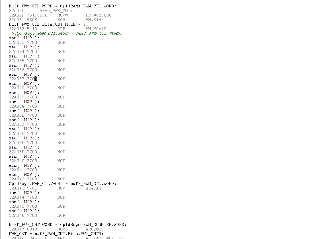
    You are right. This look strange. Look like it is something to do with CPU pipeline and for that we would need the assembly instructions for working and non-working code. Can you provide the same. Also in working case (when you have NOP) you have the write two time. Please remove one of the write (before NOP) and see if it still work and provide the assemble for that code.

    Vivek Singh
  • Hi Vivek,

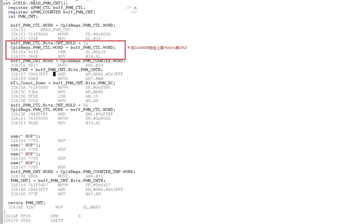
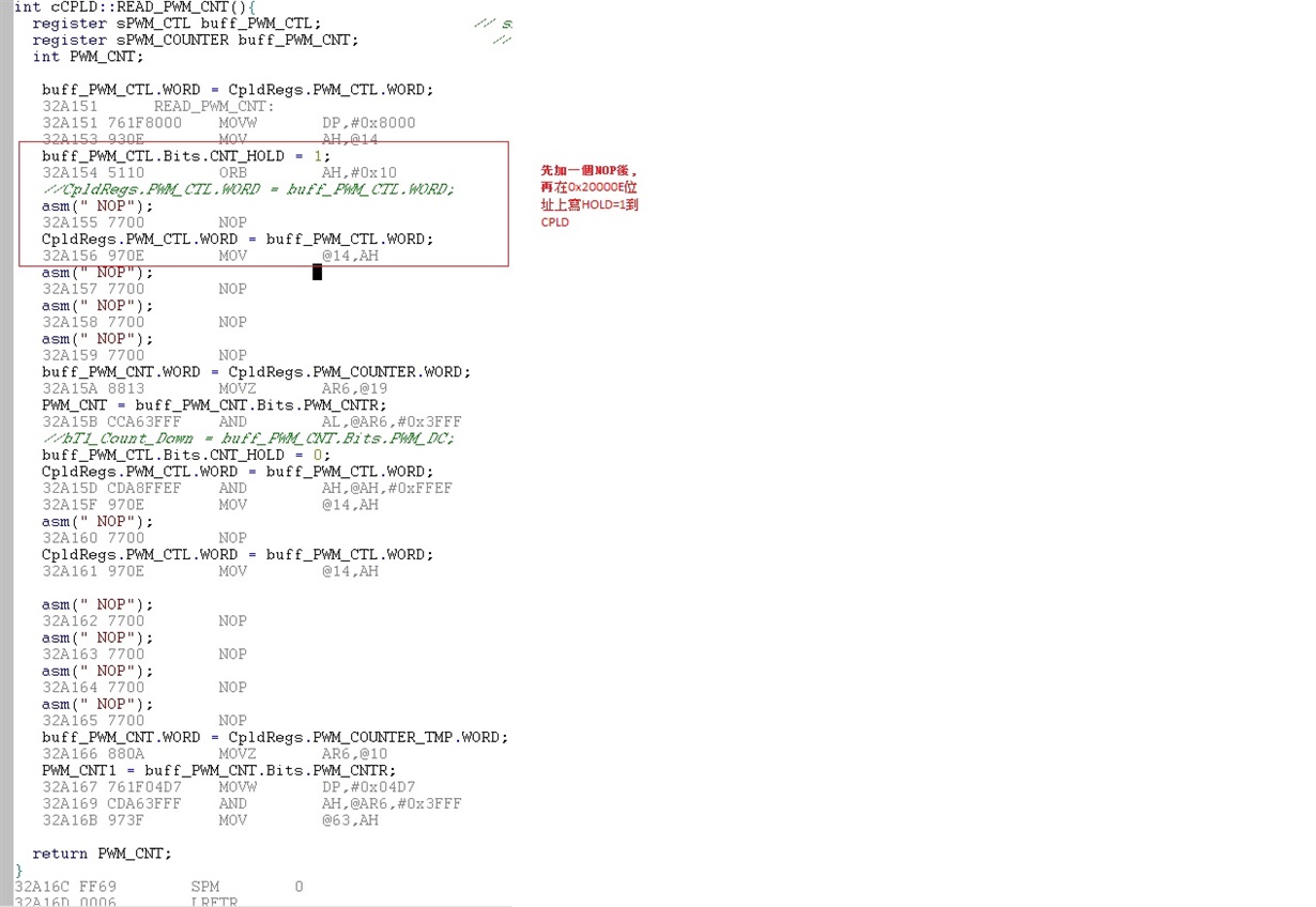
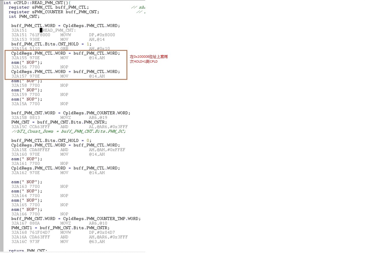
    assembly instructions for working and non-working code as below:

    Fail1- code & wave

    red text1: write HOLD=1 to CPLD at 0x20000E address

    red text2: the data should be 0x37 @(reg 14),  not 0x27.

    Fail2- code & wave

    red text1: add a  "NOP" , then write HOLD=1 to CPLD at 0x20000E address

    red text2: the data should be 0x37 @(reg 14),  not 0x27.

    pass- code & wave

    red text1:  then write HOLD=1  twice to CPLD at 0x20000E address

    red text2:1st time write @(reg 14) data is 0x27.

    red text3: waiting a  "NOP" , then write a "0x37" to @(reg 14) again, and it passes.

    best regards,

    Simen

  • Hi Vivek

    Add customer other information,

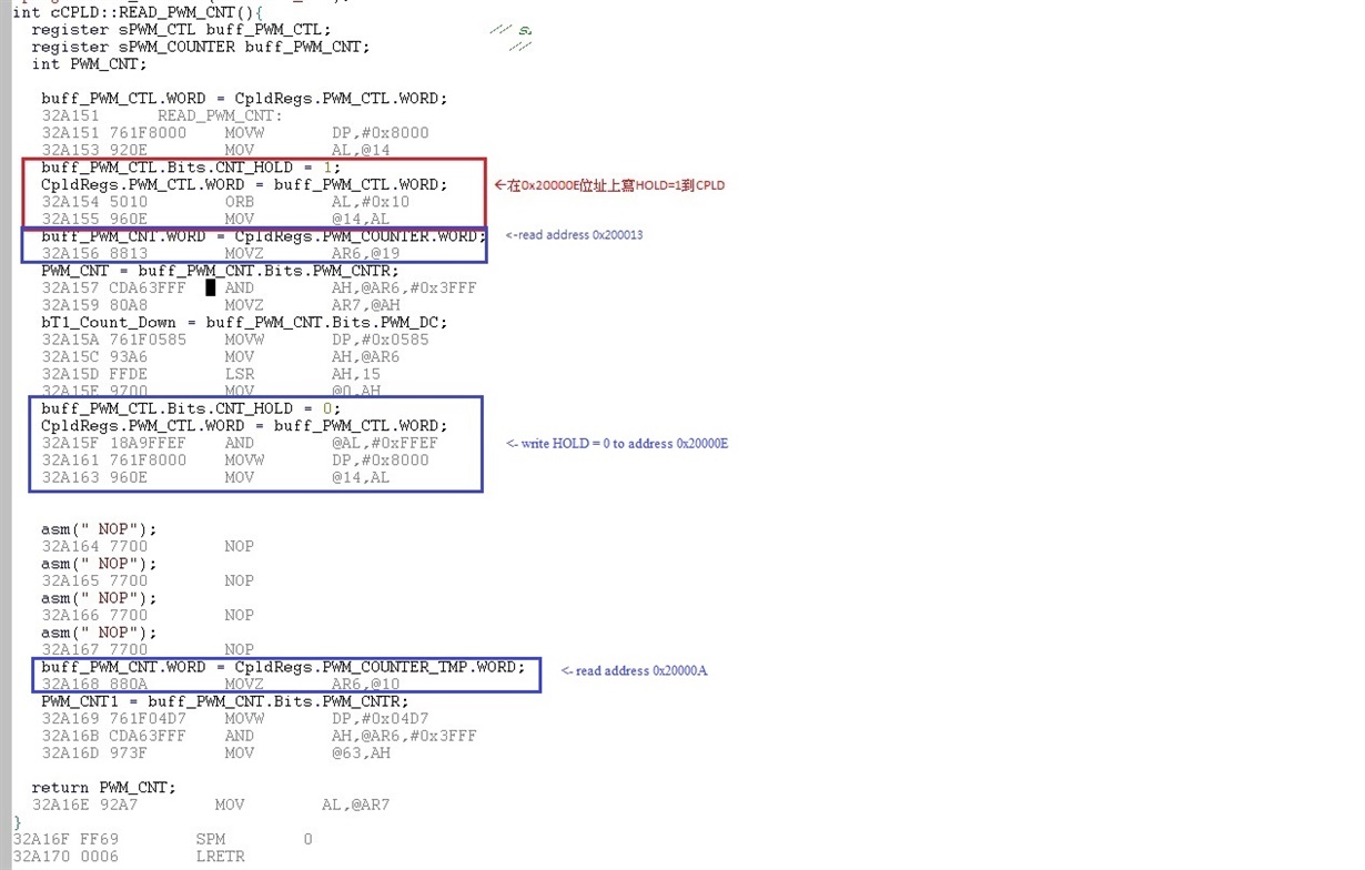
    1. Fail3 code is write/read timing wrong.

      code expect:  write reg 14 => read reg 19 => write reg 14=> read reg 10 .

     wave  result :  read reg 19 => write  reg 14 => write  reg 14 => read reg 10

    2. Fail4 Code has no effect with write and wait 16 "NOP" delay.

       But It can work when it writes twice.

    ------------------------------------------------------------------------------

    Fail3- code and wave

    Fail4- code and wave

    best regards,

    Simen

  • Hi Simen,

    Sorry for late reply. Result from Fail-3 code is expected. Reg14 and Reg19 are different address hence sequence of operation can change due to CPU pipeline. In CPU pipeline WR is last phase so if even if there RD after WR, RD can get executed before WR. Following is CPU pipeline (for more detail please refer CPU User Guide) -

    About other issue, we still have no idea why it is happening.

    Is it possible for you to provide a sample CCS project with this issue which I can use to replicate the issue here?

    Also are you using any compiler optimization? Is it possible to disable the optimization and see if it works without optimization?

    Other thing to try is after write operation to reg14, can you add read also to reg14 to see what is the value you are getting back ?

    Regards,

    Vivek Singh 

  • Hi Vivek,

    Result from Fail-3 code is expected because due to CPU pipeline =>
    1. How could I follow some rule to avoid this result?
    Because we usually need r/w XINTF in a specific order, but the sequence of operation changing will affect big trouble.
    2. Sequence of operation changing by pipeline only happened in XINTF? Does internal memory access work well?

    Thanks

  • Hi Justin,

    Because we usually need r/w XINTF in a specific order, but the sequence of operation changing will affect big trouble.


    Change in sequence should not have any impact on functionality. This is done to improve the performance. Like in this case reg19 and writing reg14 are independent action (different register) hence reg19 is read before reg14 wr. If it was write to reg14 and then readback to reg14 then the order will not change.

    2. Sequence of operation changing by pipeline only happened in XINTF? Does internal memory access work well?


    This is not limited to XINTF. It's applicable to all the address space which not pipeline protected (e.g. even internal RAM). All the peripheral space are pipeline protected so peripheral register access will follow the order. This information is available in memory map of the device.

    Regards,

    Vivek Singh
  • Hi Vivek,

    I understand your explanation. But because we use XINTF with CPLD. Due to CPLD specification, the sequence of "write reg 14/read Reg 19" can't change. I add 3 NOP after writing reg14 can make order correct. Is any better solution for this situation?
  • Justin,

    You need to insert NOP in code for this.

    Vivek Singh
  • Justin,

    Other option would be to use the XINTF "Zone 0" space for this which is protected hence will not change the sequence.

    For original failure, do you have a sample project which I can use?

    Regards,
    Vivek Singh
  • Hi Vivek,

    If we use insert NOP for sequence changing issue. How many NOP sould we insert?
    About the original failure, can you provide your email address? I will send project to you.
    Thanks
  • You'll need three NOPs.

    Vivek Singh
  • Hi Vivek,

    I have already sent project to you.
  • Hi Vivek,

    Do you have any idea after you receive our project ?
  • Hi Vivek,

    Customer has closed this issue.
    thanks,
    -----------------------------------------------------------------
    Justin check if 3 "NOP" may cause CPLD wrong work.
    And it passes the test.


    best regards,
    Simen