This thread has been locked.

If you have a related question, please click the "Ask a related question" button in the top right corner. The newly created question will be automatically linked to this question.

ADC acquisitions being missed

Guru 54057 points
Part Number: TM4C1294KCPDT
Other Parts Discussed in Thread: INA240

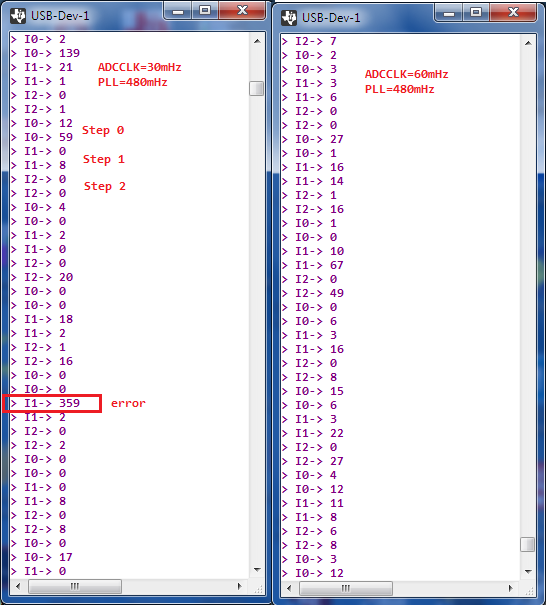
Having discovered some part of precision error ADC0 was related to periodic analog signal triggered sample step POP's into specific array cells are zero.  The digital conversion of the actual value is near 2mV analog signal yet 0x0000 was sampled. 

Speeding up ADCCLK to what is believed to be 60mHz with supposedly 480mHz PLL improves ADC sample acquisition precision. How can precision increase beyond the 2MSPS if ADCCLK being 30mHz or even 60mHz is acquisitioning far to many 0x0000 in numerous samples? The analog signal has very clean acquisition points. When sequencer is triggered via GPTM the AD converter appears to produce finer acquisition granularity locking on analog signal than being triggered via PWM0 GEN0 that is producing 80us analog signal peaks being sampled. Also the values being POP into array cells only slope the steady state signal up to a threshold (200mA) being 2mV but refuses to slope below that VREFP-VREFN value of previous POPs even though the initial slope is positive from 0v up to 2mV. If a cheap 6000 count 1.2kHz DMM can easily measure this same current (up/down) scale surly the TM4C precision ADC can easy as pie, right? This DMM by no means has such a precision ADC the TM4C is touted to have, so there must be something gone all wrong in sequencer configuration.

ADCSSFSTAT TPTR index alignment to actual POP of FIFO data has no effect to improve missing acquisitions 0x0 below. AD converter should never produce full strings of 0x0 after or during the analog signal approaching and then reaching steady state, right? AD conversion actually starts out by producing a heck of lot more strings of 0's than shown below.

It seems there is a timing issue with SYSCLK and ADCCLK being in different time domains even though supposedly VCO is producing both clocks plus the 60Mhz PWMCLK. How can a 60mHz ADCCLK even be possible without raising MCU temperature from overclocking ADC module yet here it is in the diagram below?

  • BP101,
    ADCLK of 60MHz is not supported, and therefore not worth discussing.
  • Part of the confusion to set low end of scale is 1MSPS does not improve values nor does hardware averaging, disabled above capture. The DDM measures 188mA peaking over 650mA on start up (above) but the INA240A1 should be creating 10mV/A open loop gain with 500uOhm shunt and seems to peak near 174mV or 1.74 amps. DMM measures seem to concur with Hantek CC65 current clamp measures of past tests so I trust what it shows.

    Scope 10X probe with 10X vertical attenuation shows 174mV peaks, lower than most sample digits shown above. Ideally converter decimal 22 (17.4mV) should indicate 1.74A and 174mV (17.4A) so AD converter should range near decimal 216 not so low like it does above capture.

    It seems the AD converter is not producing correct VREFP-VREFN decimals 216 and higher for 174mV input source of periodic single ended analog DC signal that may also cross zero vector in sinusoidal DC signals. Don't even care about the negative half cycle, it is unimportant in this very low measure. The AD converter seems to be subtracting VREFN-VREFP from inversion of the sinusoidal input signal, the DMM ignores.
  • Hi Bob,

    Point was it must not be 60mHz ADCCLK (PLL480/8) ADC should lock up converter other gates but it doesn't ring a bell of concern that it does not?

    So what about the very low converter values, decimal zero being repeated so often and 174mV does not produce decimal 216 from AD conversions?
  • Hi Bob,

    Our past discussion 805uV versus 201uV LSB is again front center relative to lower decimal numbers (16,18,20,59) being acquisitioned at 1MSPS or 2MSPS. If we were to assume 805uV LSB the decimal values (above) should be in 200 range for 284mV peak analog signal (below). Yet they are not in 200 decimal range, that in of it's self contradicts Fig.15-9, no matter where the analog signal is being sampled or how often, though it occurs every 80us like clock work. 

    Why do periodic ADC samples produce far less digital weights by nearly a factor of 10x? Seemingly Fig.15-9 scale 1 LSB is 201uV or lower, not 805uV as was earlier presented. If you insist 805uV LSB the scope capture and digital conversion values above seem to argue against that believed point. Signal below is similar to the M3 ADC sampling previously producing accurate ratio metric current measures from a simple OP amp converting the shunt voltage with no exotic PWM filtering the INA240 has on it's front end. That was developed at TI to work with SAR ADC, not much has changed other than the improved resolution error % from amplifier drift etc. 

    The question again is why would the digital values be so low if 805uV was intended 2MSPS? The digital values do not seem to add up to the reality of what is being sampled, acquisitioned and AD converted to digital (0-4096). The TM4C SAR seems to sample signals from VREFN up to VREFP when FIFO is drained after POP and stops at the lowest point voltage, even though Cext is charge sharing with CADC from VREFP down to VREFN. 

    No ratio metric results from draining the FIFO after sequencer step POP into C+ array and clearing the ADCOSTAT,  ADCUSTAT prior to the next POP of IE END step. Yet the low FIFO values seem to suggest 0-8096 is the +3v3 VREFA full scale perhaps not so much 4096 at 2MSPS.