Hello,
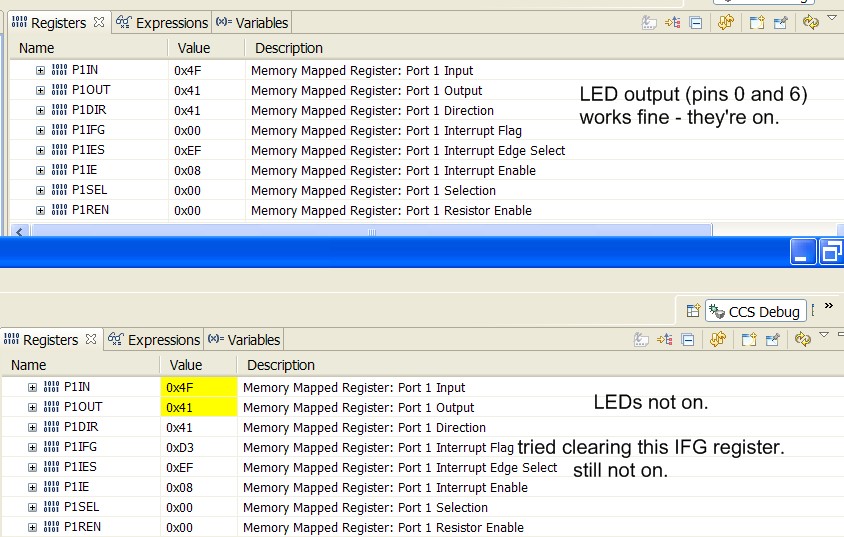
I've only done 5 or 6 MSP430 projects, so I'm pretty new, but still have never seen this before. I'm following my program in debug, and even though it's properly setting the P1OUT and P1DIR bits, I'm not getting any output at the specified pins. Does anyone know what might cause this and what can effect pin output other than the P1 registers? My code is below, as is a picture of the debugger window once when it is working and once when it's not. I saw that the only difference in the P1 registers was the interrupt flag, so I tried clearing it, but that didn't help.
Here's my code:
//***************************************************************************************
// Project:
// Chip:
// Description:
// Date:
// Created by Michael Willems
//***************************************************************************************
#include "msp430g2231.h"
// Define functional aliases.
#define MAX(a, b) a > b ? a : b // Returns the greater of a and b.
#define USE_VLO (BCSCTL3 |= LFXT1S_2) // Uses VLO for ACLK.
// Define variable aliases.
#define RED BIT0 // Pin 1.0, used for red LED and time input.
#define GREEN BIT6 // Pin 1.6, used for green LED and T-critical input.
#define BUTTON BIT3 // Pin 1.3, connected to pushbutton (which grounds).
#define SOURCE_TEMP BIT4 // Pin 1.4, will be connected through POT to the pin
// where Tcrit user input will be measured (TEMP_IN).
#define SOURCE_TIME BIT7 // Pin 1.7, will be connected through POT to provide
// controllable divider voltage at TIME_IN.
#define RESET_HOLD_TIME 10 // Defines how long button must be held for reset.
#define TEMP_IN RED // Choose red LED output pin for measuring T_CRIT.
#define TIME_IN GREEN // Choose green LED output pin for measuring TIME.
#define TEMP_CHANNEL 10 // Analog input channel 10.
#define T_BLINK 10000 // Blink period of 1000 cycles.
#define T_SAMPLE 12000 // Sampling period of roughly 12k cycles at 12kHz.
// Declare global variables.
unsigned int TEMP; // Temperature measurements stored here.
unsigned int TIME; // Time threshold (acceptable overage) stored here.
unsigned int T_CRIT; // Critical temperature stored here.
unsigned int OVERAGE; // Stores the total time*temp over the limit.
int WAKEUP_NEXT; // Flag used by the button ISR to either wake or sleep.
int T_CRIT_SET; // Flag ensures ADC only sets critical temp once.
int TIME_SET; // Flag ensures ADC only sets time threshold once.
//***************************************************************************************
// FUNCTION DEFINITIONS
//***************************************************************************************
/*
* This function configures the ADC to read off of 2 P1 inputs, takes voltage readings,
* and stores the results in the TIME and T_CRIT fields for further use.
*/
void readThresholds(void)
{
/******************** READING T_CRIT ********************/
// Configure measurement pin as inputs with internal pull up resistors off.
P1REN &= ~(TEMP_IN); // Pull-up resistors off for measurement pins.
P1OUT &= ~(TEMP_IN); // Turn off output before switching to input.
P1DIR &= ~(TEMP_IN); // Can be input or output, ADC doesn't care.
// Thus, set direction to input with resistors off so it won't get set hi or lo.
// Configure ADC channels to read POT-divided voltage at T_CRIT input first.
ADC10AE0 |= TEMP_IN; // Make T_CRIT input pin analog to make available to ADC.
ADC10CTL1 = TEMP_IN; // Set ADC to read from T_CRIT input pin.
// Enable ADC10 interrupt, set reference voltages, and turn ADC on.
ADC10CTL0 = SREF_0 + ADC10SHT_2 + ADC10ON + ADC10IE + REFON + REF2_5V;
// Turn on supply voltage for T_CRIT voltage divider.
P1DIR |= SOURCE_TEMP; // Set T_CRIT divider source to output.
P1OUT |= SOURCE_TEMP; // Turn divider source on.
// Start read.
ADC10CTL0 |= ENC; // Enable conversion bit set.
ADC10CTL0 |= ADC10SC; // Start conversion bit set.
//Wait in LPM3 with everything off except ACLK (VLO) while ADC writes data.
_BIS_SR(CPUOFF + SCG1 + SCG0 + GIE); // Enter LPM3 w/ interrupt.
// Read ADC10 in ISR. ISR will return here.
/******************** READING TIME ********************/
// Turn off supply to Temperature voltage divider and reset to output.
P1OUT &= ~SOURCE_TEMP;
P1DIR += TEMP_IN;
P1OUT |= TEMP_IN;
// Configure measurement pin as inputs with internal pull up resistors off.
P1REN &= ~(TIME_IN); // Pull-up resistors off for measurement pins.
P1OUT &= ~(TIME_IN); // Turn off output before switching to input.
P1DIR &= ~(TIME_IN); // Can be input or output, ADC doesn't care.
// Thus, set direction to input with resistors off so it won't get set hi or lo.
// Now configure ADC channels to read POT-divided voltage at Time input.
ADC10AE0 |= TIME_IN; // Enable Time input pin as analog to make available to ADC.
ADC10CTL1 = TIME_IN; // Set ADC to read from Time input pin.
// Enable ADC10 interrupt, set reference voltages, and turn ADC on.
ADC10CTL0 = SREF_0 + ADC10SHT_2 + ADC10ON + ADC10IE + REFON + REF2_5V;
// Turn on supply voltage for Time voltage divider.
P1DIR |= SOURCE_TIME; // Set Time divider source to output.
P1OUT |= SOURCE_TIME; // Turn Time divider source on.
// Start read.
ADC10CTL0 |= ENC; // Enable conversion bit set.
ADC10CTL0 |= ADC10SC; // Start conversion bit set.
//Wait in LPM3 with everything off until ADC complete interrupt wakes up.
_BIS_SR(CPUOFF + SCG1 + SCG0 + GIE); // ACLK runs ADC while it converts result.
// Read ADC10 in ISR. ISR will return to here but awakened.
// Disable ADC to save power and so control bits can be changed next time.
ADC10CTL0 &= ~ENC;
// Turn off supply to Temperature voltage divider and reset to output.
P1OUT &= ~SOURCE_TIME;
P1DIR += TEMP_IN;
P1OUT |= TEMP_IN;
// Calculate the overage limit as a function of the TIME raw input data, and store
// that result as the variable to compare to:
TIME = TIME >> 6;
return;
} //*************************************************************************************
//***************************************************************************************
/*
* This function blinks the green LED once for roughly T_BLINK cycles.
*/
void blinkGreenOnce(void) {
P1DIR = GREEN;
P1OUT = GREEN;
long i;
for(i = T_BLINK; i>0; i--);
P1OUT &= ~(GREEN);
} //*************************************************************************************
//***************************************************************************************
/*
* This function blinks the red LED once for roughly T_BLINK cycles.
*/
void blinkRedOnce(void) {
P1DIR = RED;
P1OUT = RED;
long i;
for(i = T_BLINK; i>0; i--);
P1OUT &= ~(RED);
} //*************************************************************************************
//***************************************************************************************
/*
* This function blinks both LEDs once for roughly T_BLINK cycles.
*/
void blinkBothOnce(void) {
P1IFG = 0;
P1DIR = RED + GREEN;
P1OUT = RED + GREEN;
long i;
for(i = T_BLINK; i>0; i--);
P1OUT &= ~(RED + GREEN);
} //*************************************************************************************
//***************************************************************************************
/*
* This function takes one integer parameter, period, and sets up the ADC and a VLO clock
* to take readings roughly every [period] seconds.
*/
void setTemp(void) {
//Disable ADC so control bits can be changed.
ADC10CTL0 &= ~ENC;
// Configure ADC channels to read internal temperature sensor.
ADC10CTL1 = TEMP_CHANNEL; // Set ADC to read from Time input pin.
// Enable ADC10 interrupt, set reference voltages, and turn ADC on.
ADC10CTL0 = SREF_0 + ADC10SHT_2 + ADC10ON + ADC10IE + REFON + REF2_5V;
// Start read.
ADC10CTL0 |= ENC + ADC10SC; // Enable and start conversion bits set.
//Wait in LPM3 with everything off until ADC complete interrupt wakes up.
_BIS_SR(CPUOFF + SCG1 + SCG0 + GIE); // ACLK runs ADC while it converts result.
// Read ADC10 in ISR. ISR will return to here but awakened.
// Upon exit, disable ADC to save power and so control bits can be changed next time.
ADC10CTL0 &= ~ENC;
} //*************************************************************************************
//***************************************************************************************
/*
* This function starts the main method again - rereading threshold settings.
*/
void reset(void) {
// Writing to the p/w protected WDT control without p/w causes reset.
WDTCTL = WDTHOLD;
} //*************************************************************************************
//***************************************************************************************
// MAIN FUNCTION
//***************************************************************************************
/*
* This is the main function.
*/
int main(void)
{
// Basic setup: // Initialize global variables.
TEMP = TIME = T_CRIT = WAKEUP_NEXT = OVERAGE = T_CRIT_SET = TIME_SET = 0;
WDTCTL = WDTPW + WDTHOLD; // Stop WDT
USE_VLO; // Configure VLO as ACLK.
// Enable button interrupts (for sleep and reset):
P1IE |= BUTTON; // Enable button interrupts (also necessary).
P1IFG &= ~BUTTON; // Clear button interrupt flag.
_BIS_SR(GIE); // Enable general interrupts.
P1DIR |= RED + GREEN; // Debug - turn LEDs to output.
P1OUT |= RED + GREEN;
// Measure and set T_CRIT and TIME:
readThresholds();
blinkBothOnce(); // Blinks LEDs once to signify proper reset / read on settings.
// Configure timer:
TACCR0 = T_SAMPLE; // Configure the Timer A count limit.
TACCTL0 |= CCIE; // Enable timer interrupt.
TACTL = TASSEL_1 | MC_1; // Configure Timer A to use ACLCK and start it.
_BIS_SR(CPUOFF + SCG1 + SCG0 + GIE); // Enter LPM3 w/ interrupts enabled.
} //*************************************************************************************
//***************************************************************************************
// INTERRUPT SERVICE ROUTINES
//***************************************************************************************
/*
* Timer A0 interrupt service routine. Gets called periodically about once a second.
* This routine must perform the temperature measurements and processing.
*/
#pragma vector=TIMERA0_VECTOR
__interrupt void Timer_A_ISR (void)
{
if(OVERAGE > TIME){
blinkRedOnce();
} else {
setTemp();
if(TEMP > T_CRIT){
OVERAGE += TEMP - T_CRIT;
blinkRedOnce();
} else { // temp <= critical temp
blinkGreenOnce();
}
}
}
/*
* ISR for button push interrupt. Every other (odd) push triggers sleep in LPM4
* (turns the device off). Even button pushes cause a software reset, beginning
* with new input read.
*/
#pragma vector=PORT1_VECTOR
__interrupt void Button_ISR(void)
{
if(WAKEUP_NEXT)
{
//Waking up.
WAKEUP_NEXT = 0; // Should be done by MCU on reset anyway, but to clarify.
P1IFG &= ~BUTTON; // Clear push button Interrupt Flag.
reset(); // POR reset restarts main function.
}
else
{
//Turning off and going to sleep.
P1OUT = 0; //Turn off all outputs.
WAKEUP_NEXT = 1; // Next button push wakes up.
P1IFG &= ~BUTTON; // Clear push button Interrupt Flag.
_BIS_SR(CPUOFF + OSCOFF + SCG1 + SCG0 + GIE); // Enter LPM4 w/ interrupt.
}
}
/*
* Interrupt for the ADC10. Either reading voltage or temperature, must account for both.
*/
#pragma vector=ADC10_VECTOR
__interrupt void ADC10_ISR(void)
{
if(T_CRIT_SET && TIME_SET) { // If both are set, then we're taking temperature.
TEMP = ADC10MEM;
} else {
if(!T_CRIT_SET) { // T_CRIT will be set first.
T_CRIT = ADC10MEM;
T_CRIT_SET = 1;
} else { // Then TIME is set if T_CRIT has already been set.
TIME = ADC10MEM;
TIME_SET = 1;
}
}
// Clear CPUOFF bit from 0(SR) to stay awake and finish function.
__bic_SR_register_on_exit(LPM3_bits);
}