This thread has been locked.

If you have a related question, please click the "Ask a related question" button in the top right corner. The newly created question will be automatically linked to this question.

Project: create an analog signal using MSP430G2553

Other Parts Discussed in Thread: MSP430G2553

Hello, I'm Antonis (I'm studying Automation Engineering in Thessaloniki, Greece)

It' s my first post here  and  I really need your help

First, of all this project -> to create an analog signal was my idea

My professor told me that this project should be done with that micro-controller (MSP430G2553).

So my thinking is to 

1. input 12bit from deep switch ->use them as a StartingNumber

2. these 12bit StartingNumber to increase till reaches 2^12 (=4096)

3. then decrease till 0. This way to create a digital triangle signal

4. that digital signal goes to a DAC7611p , so to output an analog signal

On  CCS, 

void main (void)

{

  WDTCTL=WDTPW+WDTHOLD; 

  P1DIR &=~ 0xFF; //input Port1

  P2DIR &=~ 0x78; //input P2.3-P2.6,  so 12 bits input

  P2DIR |= 0x07;  //Output P2.0-P2.2

  P1REN |=0xFF;  //enable pull-up resistor 

  P2REN |= 0x78;

// using FOR or WHILE to increase till 4095, maybe something like  while((P1IN!=0xFF) && (P2IN!=0x78))

  {StartingNumber++;}

// now another to FOR or WHILE to decrease

  {StartingNumber--;}

If you have anything to propose, anything that I need to read (apart from data sheets, that I already did), would be thankful !

  • Hi,

    Seems like you have the right idea.

    When the micro starts up though, all general purpose input/output pin directions are set as inputs.  This is the 'safe' way, to prevent them perhaps driving things they shouldn't.  You don't need to set the pins as inputs as your first task.  Although it shouldn't hurt to do so.

    Statements like 'x &= ~y' and 'x |= y' modify the current value of x.  If that were a port direction register, it would mean "take the value in the port direction register that it has now, and modify some of the bit values (although some might be all of them depending on what y is)"  If you know how you want the pins set up, you can just assign them with an equals sign:

    P1DIR = 0x00;   //all port 1 as inputs, which they are anyway

    P2DIR = 0x87;  //port 2 bits 0,1,2 and 7 as outputs - they will initially drive low as P2OUT starts up as 0x00

    You haven't mentioned about the DAC - is it a parallel one?  You'll need to connect this to some port pins too.

    For the heart of the code, you firstly need to read the DIP switch setting by reading the values on the input pins.

    As the MSP is a 16 bit device and ports are only 8 bits wide, you'll have to do this in two chunks to read 12 bits, then stitch them together to get a 12 bit number:

    unsigned int temp1, temp2, result;

    temp1 = P1IN;   //read the value of the 8 pins on Port 1 into the lowest 8 bits of temp1

    temp2 = P2IN;   //read the value of the pins on Port 2 (all of them including the output pins) into lowest bits of temp2

    You'll then need to manipulate the bits in temp1 and temp2 to create 'result', which has the bits where you need them.  This will depend on whether the DIP switch Least Significant Bit is connected to Port1 or Port2, and whether it is the lowest number bit used in that port or the highest bit.  Something like:

    result = (temp2 & 0x78);   //leave only the bits we are interested in set if they read high.  Zero non-used bits

    result = result << 5; // the lowest bit of interest (bit 3) needs to become bit 8, to make room for lowest 8 bits

    result = result | temp1;  //any bits in temp1 that read as set now go into the lowest 8 bits of the number.

    You now have 'result' holding 12 bits of the DIP switch.  You can do all this in one line as:

    result = ((temp2 & 0x78) << 6 ) | temp1;

    But make sure you think through the individual actions of each part and use brackets to constrain the order of execution.

    You can now start to increment or decrement 'result' and output the values to the DAC.

    Hope that helps.

  • Hey Tony,

    I apologise for not replying earlier,

    Two days ago I tried your  commands

    WDTCTL=WDTPW+WDTHOLD;

    P1DIR = 0x00;  

    P2DIR = 0x87; 

    unsigned int temp1, temp2, result;

    result = (temp2 & 0x78); 

    result = result << 5;

    result = result | temp1; 

    //afterwards for decrement & increment

    while(result >=0 && result<=4095){

             result++;

    }

    while(result >=0 && result<=4095){

             result--;

    }

    I used oscilloscope , but there was NO frequency of my circuit.

    I connected the DIP switch - with MSP430g2553 - with the PARALLEL DAC7611p 

    Output of that circuit was 3 Volt DC

    Although I wanted an analog triangle 0-3 V. 

    I believe that there must be some commands on frequency.

    Maybe I made some mistakes on increasing/ decreasing the RESULT

    What do you say ?

    Thanks a lot

  • Do you mean using 12 DIP (Dual Inline Package) switches just to manually set up the initial value of StartingNumber?

    That seems to be much ado about almost nothing. Why not just from 0 up to 4095 and down to 0? As a matter of fact, I think you could repeat that in an endless loop.

    while (1)
    {
      for (value = 0; value < 4095; value++)
      {
        send_to_adc(value);
        load_adc();
      }
      for (value = 4095; value > 0; value--)
      {
        send_to_adc(value);
        load_adc();
      }
    }

  • Antonios Katsikinis said:
    4. that digital signal goes to a DAC7611p , so to output an analog signal

    You can also generate an analogue signal by using a timer to create a PWM pulse and output this to an RC network, instead of using a DAC.

  • Antonios

    Glad to see you are still working on this.

    There are a number of things that I believe you will have to work on, breaking the problem up into smaller chunks and working on each bit separately may well help and will allow you to prove that one bit works before working on the next.  This will also make it easier to see, if things don't work as expected, where the problem is.

    I checked the data sheet of the DAC7611P and it said it is a serial (not parallel) 12-bit DAC having 8 pins.  If this is the same as the one you are using, you will need to consider how to send serial data (plus a couple of control signals) to that chip.  Parallel DACs usually have one pin per bit, e.g. for 12 bit DAC then a parallel DAC would have 12 pins for the data, plus at least one control pin (to tell it when to read and apply the new value) plus perhaps a chip select pin plus a couple of power pins, as a minimum.  So a 12 bit parallel DAC is going to need at least 15 pins.  If it has less than this, it is probably a serial DAC.

    I'd suggest you leave the DIP switch until you've got the DAC working.  Once you know that you can send any value to the DAC, it should be a lot easier to implement the DIP switch.  Are you restricted to using the DAC7611P or can you use another method, perhaps such as the one Leo suggests, or perhaps using an R2R ladder (look this up on internet if you are not familiar with it, it is a kind of home-made parallel DAC)?

    You need to decide about controlling the DAC to obtain the analogue output first.  You can generate any number in code to check if the DAC works.  But if the DAC isn't correctly outputting the values you generate, you will not know if the problem is in the number calculation routines, the DIP switch reading routines or in the DAC control routines.

    Can you check your data sheet for the DAC and confirm if it is serial or parallel?  And how do you intend to signal to it - which port pins from the microcontroller will connect to which DAC pins?

    Tony

  •  Hi, some analysis necessary:

    Antonios Katsikinis said:

    1. input 12bit from deep switch ->use them as a StartingNumber

     You mean DIP switch? use program instead, is more simple to control.

    Antonios Katsikinis said:
    4. that digital signal goes to a DAC7611p , so to output an analog signal

     This appear as a serial SPI like expensive DAC, are you owning it? Otherwise another better  chip or PWM can be used instead.

     Nothing is defined about what are your goal, so resolution and bandwidth of signal, again some part like MSP430F26x carry two 12 bit DAC onboard and chip is costing less than DAC itself.

    see there for a dev board

    https://www.olimex.com/Products/MSP430/

     or launchpad using MSP430G2553

     If you own the dac a driving routine is needed SPI based or Bit banging to transfer data to DAC.

  • Thank you,

    all of you for replying to my post, 

    I own MSP430g2553 and DAC7611p. 

    I made some mistakes. DAC7611p is a SERIAL DAC (12 bits- 8 pins) as Tony said.

    I 'll leave the DIP switch and use program (a lot easier). So my program will change a little.

    Before some years I did use the R2R (ladder), although now I prefer to use the DAC.

    I used as input to the pin (SDI - Serial Data Input) of DAC7611p , the output of MSP430.

    SO NOW my issue, what is needed, is to program MSP430 to create a signal 

    my thinking is to create a digital signal which will move from 0 to 3 V and back (from 3 to 0)

     that will be inserted to the DAC and the result should be an analog signal , between 0 -3 V.

    I don' t know about the frequency

    also don' t know, while changing the bits from 0000 to 4095 (2^12), if the voltage changes from 0 to 3

    thank you

    Antonis

  • Antonios Katsikinis said:

    I don' t know about the frequency

    also don' t know, while changing the bits from 0000 to 4095 (2^12), if the voltage changes from 0 to 3

     Ok Try a step by step..

     What is the goal of your project so what you think to realize and what you expect to do? This can help us understand better solution.

     Other, Hardware SPI or Bit Bang?

     Bit bang

    Use as much as possible predefined constant than number.

     On header BIT0 to BITxx are predefined as 01 02 04 08.... and are more readable than an hex number.

    use shift left n bit  <<n  or shift right n bit >>n

     no time constraint never if cpu at full speed than data hold.

    Init interface:

     Set CS high

    Set Clk High

    Set LD High

     Move data:

    Set CS low

    for (12 times)

           Set clock low

            copy bit 11 of DAC value to data pin

            set CLK High

            Shift Dac value left

    Now set CS High

    Set LD Low

    Set LD High

    //********************************* Code BIT BANG ************************************************************

    /* enjoy this code and call as OCY show you.. Just customize for pin

     Biggest data or clock setup is 30nS, instruction time @16Mhz is 62.5nS so we don't worry about...

     Customize x, z etc to your port number, bit y k etc to bit number of your port and extend macro to all oher  CLR LD

    */

    #define CS_LO (PxOUT&=~BITy)

    #define CS_HI (PxOUT|=BITy)

    #define SDI_LO (PzOUT&=~BITk)

    #define SDI_HI (PzOUT|=BITk)

    .........

    void send_to_adc(value)

    { int i;

      CS_LO;

      for(i=0;i<12;i++)

      {

         CLK_LO;

         if(data&BIT11) // out MSB first

             SDI_HI;   // data bit is 1

          else

              SDI_LO;  // data bit is 0

          data<<1; // shift  left data

          CLK_HI;

      }

      CS_HI;

    }

    void load_adc(void)

    {

      LD_LO;

      LD_HI;

    }

    // call this before the other just after setting Watchdog and port direction

    void Initadc(void)

    {

    CS_HI;

     LD_HI;

    }

  •  Hi again, i leave this separate to not overload...

    Antonios Katsikinis said:
    also don' t know, while changing the bits from 0000 to 4095 (2^12), if the voltage changes from 0 to 3

    Inserrt function code before main or use forrward header declaration

    init_ADC(); // set adc pin level...

     // this set dac value to 0

        send_to_adc(0);
        load_adc();
    // this set dac value to full scale

        send_to_adc(4095); // oxffff set full scale too but limited to 0X0FFF by resolution
        load_adc();

    // this set to middle of FS value

        send_to_adc(2047);
        load_adc();

    Other value set to

      FS*value/4095

     FS is 212-1 and not 212

    unsigned MAxint in general is 2n-1

    if singed MAXINT is 2n-1-1 accounting the sign bit.


  • I wanted to upload my "plan"

    I'm planning NOT to use the DIP switch, as you proposed me.

    So everything I need is to 

    CREATE AN ANALOG SIGNAL. It would be better if that signal will be triangle.

    Roberto, thank you for uploading your thinking.

    But I don' t know the differences between bit bang and SPI and I'm a little confused.

    And really need to finish this project till Wednesday.

    Thanks alot

    Antonis

  • Antonios Katsikinis said:

    But I don' t know the differences between bit bang and SPI and I'm a little confused.

     Bit Bang is a software SPI, spi mean Serial Peripheral Interface, coming from early age of microcontroller, formerly from Motorola (now freescale) and grown to every manufacturer. Many variantr exist in particular about clock initial phase, data load clock edge and timing.

     Anyway from your wiring Hardware SPI are not available to pin of P2 both are on P1, other than rewire use the proposed code as is.. so customize it and use

    #define CS_LO (P2OUT&=~BIT3)

    #define CS_HI (P2OUT|=BIT3)

    #define SDI_LO (P2OUT&=~BIT1)

    #define SDI_HI (P2OUT|=BIT1)

    #define CLK_LO (P2OUT&=~BIT2)

    #define CLK_HI (P2OUT|=BIT2)

    #define LD_LO (P2OUT&=~BIT0)

    #define LD_HI (P2OUT|=BIT0)

     From your drawings no CS signal is provided, SPI cannot work without this signal so disconnect IE P2.3 ans wire to pin 2 of dac.

     Anyway compiling the code you got fronm sunday it can be working. The worst wednesday is tomorrow.. Is crazy ask in a so short time and try also a simple project without enough knowledge to do it..

     Never do many thing at same time so....

     When AND ONLY WHEN  code and hardware is is ok you can SAVE all, 

     then start a new project code, simply try a rewire of DAC to one of two  hardwareSPI on port P1 then enjoy faster data transfer to DAC, your actual dac has 7uS of settling time, software routine transfer a work in an approximate 50-100 cycles of clock, SPI can transfer in about 36 cycles, @16MHz you get an approximate sample freq of at least 160KHz, your triangle freq is Fx/nsamples so 160/8192 -> 20Hz

     If you wish do something different it is better to do scaling, offset and frequency control.

     Remember your dac just has 7uS settling time and triangle is worst than square and sine, it require at almost 100 time the bandwidth of fundamental frequency so 1KHz triangle require a fast  OPAMP no more a trouble these day.

     Good luck and prepare you about exam otherwise this is not your work, getting help require understand in detail.

  • Antonios Katsikinis said:

    On  CCS, 

    void main (void)

    {

      WDTCTL=WDTPW+WDTHOLD; 

      P1DIR &=~ 0xFF; //input Port1

      P2DIR &=~ 0x78; //input P2.3-P2.6,  so 12 bits input

      P2DIR |= 0x07;  //Output P2.0-P2.2

      P1REN |=0xFF;  //enable pull-up resistor 

      P2REN |= 0x78;

     Change as:

      P1DIR = 0;   //input Port1

      P2DIR = BIT0 | BIT1 | BIT2 | BIT3;  //input P2.3-P2.6,  Out bit 0..3

     P1OUT = 0xff; // required by next instruction to pullup/pulldown

     P1REN =0xFF;  //enable pull-up resistor 

     P2OUT = 0xff; // required by next instruction to pullup/pulldown and init SPI too

      P2REN |= 0xf0;

     // add here the code proposed and I think you are in a hurry with your triangle wave generated. All processor pin are in a stable configuration safe still if DIP sw are in place.

     I suggest use the launchpad button and led to do a selection of two or more frequency using the leds as display value... as you learn you can add but this require time.

  • I did whatever you told me

    I debugged it on CCS. There' s 1 mistake 

    here : if(data&BIT11) // out MSB first

    it says -> undefined data and undefined bit11

  • Antonios Katsikinis said:
    here : if(data&BIT11) // out MSB first

     Sorry, you are beginner C programming ;)

    change

    void send_to_adc(value)

     To

    void send_to_adc(int value)


    then change data to value on offending line

    Antonios Katsikinis said:
    here : if(data&BIT11) // out MSB first

    Now check all header are in place before main, BIT definition are generally in MSP430.h I try'd run and oh.. BIT XX are changed by hex value letter :( Uh.. this can be a big issue dealing to old style code...

    if(value&BITB)

     Devil is forever online :(

  • Antonios Katsikinis said:
    it says -> undefined data and undefined bit11

     When is solved please tell us and mark post as verified to give thank for time to your problem.

  • Antonios Katsikinis said:
    I did whatever you told me

     All is ok? What about your project? Just a simple step?

     Check also this, I suppose you can get some hint.

    http://e2e.ti.com/support/microcontrollers/msp430/f/166/t/344292.aspx

  • thank you very much

    well, code had no mistake although while debugging, there are 3 errors

    I couldn't load our code to msp430

    Now I need to study 2 courses.

    I will continue with this project after 26 June

    I' ll let you know here thanks a lot

  • Antonios Katsikinis said:
    I couldn't load our code to msp430

     Depending on what IDE are you using open configuration and set FET to what are you using, I suppose launchpad so this is recognized as USBFET..

  • Hello

    I' m back again to build this project right !!!

    The program is "due to" Roberto Romano

    #include <msp430.h>

    #define CS_LO (P2OUT&=~BIT3)

    #define CS_HI (P2OUT|=BIT3)

    #define SDI_LO (P2OUT&=~BIT1)

    #define SDI_HI (P2OUT|=BIT1)

    #define CLK_LO (P2OUT&=~BIT2)

    #define CLK_HI (P2OUT|=BIT2)

    #define LD_LO (P2OUT&=~BIT0)

    #define LD_HI (P2OUT|=BIT0)

    void send_to_adc(int value)

    { int i;

    CS_LO;

    for(i=0;i<12;i++)

    {

    CLK_LO;

    if(value&BITB) // out MSB first

    SDI_HI; // data bit is 1

    else

    SDI_LO; // data bit is 0

    value<<1; // shift left data

    CLK_HI;

    }

    CS_HI;

    }

    void load_adc(void)

    {

    LD_LO;

    LD_HI;

    }

    // call this before the other just after setting Watchdog and port direction

    void Initadc(void)

    {

    CS_HI;

    LD_HI;

    }

    int main(void)
    {
    WDTCTL = WDTPW | WDTHOLD; // Stop watchdog timer

    P1DIR = 0; //input Port1

    P2DIR = BIT0 | BIT1 | BIT2 | BIT3; //input P2.3-P2.6, Out bit 0..3

    P1OUT = 0xff; // required by next instruction to pullup/pulldown

    P1REN =0xFF; //enable pull-up resistor

    P2OUT = 0xff; // required by next instruction to pullup/pulldown and init SPI too

    P2REN |= 0xf0;

    Initadc(); // set adc pin level

    // this set dac value to 0

    send_to_adc(0);
    load_adc();
    // this set dac value to full scale

    send_to_adc(4095); // oxffff set full scale too but limited to 0X0FFF by resolution
    load_adc();

    // this set to middle of FS value

    send_to_adc(2047);
    load_adc();

    }

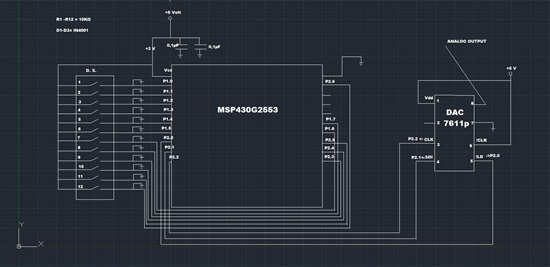
    my plan is this

    6786.TELIKO_PLANO.pdf

    I run this on Code Composer Studio v5.5 

    build -no errors -few warnings

    debug -> run ... 

    checked the oscillator for frequency, but I only got Voltage ( DC Voltage before my DAC, no freq)

    any idea ???

    Should I change the "thesis" of any Jumper ?

    Should I solve the warnings ?

    On my MSP430G2553, my experience is poor. I run the example programs, without a problem, BUT need your help here !

  • Antonios Katsikinis said:
    value<<1; // shift left data

     Antonios, a lot of time elapsed but still you are at same BEGINNER LEVEL!!!!

     YOU MUST LEARN PROGRAMMING BEFORE TO DO SIMPLE THINGS!!!!!!!


     again the warning come from a mistyped line:

    Antonios Katsikinis said:
    value<<1; // shift left data

    this must be

    value=value<<1;

    or in compact form

    value>>=1; edit :  value<<=1;

     Without this data don't load on dac and just bit 11 set all bit. This must output at almost a square wave

     I cannot help you solving your problem, you got too much so PLEASE learn c programming at a decent level otherwise you cannot get nothing and automation require good knowledge of both Mathematics and programming!

  • Antonios Katsikinis said:

    my plan is this

    6786.TELIKO_PLANO.pdf

     If you power <MSP430G2553> @ 5V I fear it burn after short time.

     In the past some of my processor due to defect on pcb got powered much more but this is not a rule, MSP MUST be run from 1.8 to 3.6V with ABSOLUTE MAXIMUM @4.1 V.


  • You are right

    I' m using 3 rectifier diodes IN0001

    So no to have voltage over 4.1

    Although I Forgot to draw it in my plan !!! 

  • The problem with rectifier diodes is that their forward voltage depends on current. MSP is low current, so diode voltage drop is low too. Well, as soon as the MSP starts to break down, current will increase and so does the diode voltage, keeping the MSP at the edge between life and death :)

**Attention** This is a public forum