This thread has been locked.

If you have a related question, please click the "Ask a related question" button in the top right corner. The newly created question will be automatically linked to this question.

Need help on configuring port 2.6 as input(MSP430G2231

Other Parts Discussed in Thread: MSP430G2231

Hi 

I require that the port 2.6 of MSP430G2231 microcontroller should be configured as input for a switching application. The whole idea is to detect a high or a low. When a high is detected(3.3V), I set a flag G_Charge_Start=1, if a low is detected(i.e 0V) I set G_Charge_Start=0. How ever I find that the P2.6 is always detecting a high in-spite of the switch on my application being low. The reason being by default when no voltage is applied to pin 2.6, I see that a 1.2-1.5V can be detected at port 2.6. But when I Isolate the controller from my application I see that on my hardware board the is no voltage (0V) when my switch is turned off. the 1.2V-1.5V is from my controller.Can somebody tell me if I have configured the ports correctly. I have pasted my code below. Please give me some suggestions. Thanks in advance.

int main(void) {
WDTCTL = WDTPW | WDTHOLD; // Stop watchdog timer
// INIT_PORTS();
P2IN&=~BIT6;
//P1DIR|=BIT0;
//P1OUT&=~BIT0;
while (1)
{
// battery_voltage = analogRead(port1);
if (P2IN & BIT6){

G_Charge_Start=1;

} else if( !(P2IN & BIT6)) {
G_Charge_Start=0; 
}

}
}


  • HI,

    It is not clear from your post quite how your switch is connected. It could be connected to Vcc or 0V. You also do not mention if you have a pull-up or pull-down external resistor.

    Assuming you have no external resistor you need to enable the internal resistor.

    For switch connected to Vcc you need.

    P2DIR &= ~BIT6;   // Set port to input
    
    P2OUT &= ~BIT6;  // Set up for Pull down resistor
    
    P2REN |= BIT6; // Enable internal resisor
    

    For switch connected to Vcc you need.

    P2DIR &= ~BIT6;   // Set port to input
    
    P2OUT |= BIT6;  // Set up for Pull Up resistor
    
    P2REN |= BIT6; // Enable internal resisor

    Then enter your while loop

    Regards

     Roy

  • Hi Roy

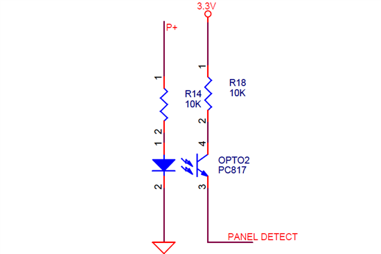
    Thank you for your reply. The code you have posted is help-full. There has been an improvement in my results. After pasting your code for 'Set up for Pull down resistor' I am no longer getting a 1.5V at 2.6 when the switch is off. However my code is detecting a high always, i.e G_Charge_Start is always 1, inspite of turning off the switch. I have also attached my switching circuit along with this post. In the diagram when P+ is high(when external switch is turned on) panel detect presents 3.3V to Port2.6. Else no voltage present at panel detect. My code now looks like the one pasted. And also find attached the switching CKT 

    int main(void) {
    WDTCTL = WDTPW | WDTHOLD; // Stop watchdog timer
    // INIT_PORTS();
    P2DIR &= ~BIT6; // Set port to input

    P2OUT &= ~BIT6; // Set up for Pull down resistor

    P2REN |= BIT6; // Enable internal resisor
    while (1)
    {
    // battery_voltage = analogRead(port1);
    if (P2IN & BIT6) {
    G_Charge_Start=1;
    } else if( !(P2IN & BIT6)) {
    G_Charge_Start=0; // ... else turn it off.
    }

    }
    }


  • Hi,

    Currently you have

    :

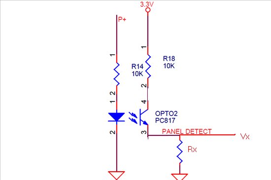
    Rx is the pull down resistor, and Vx is the actual voltage at the pin. Hence there is a potential divider between R18 + on resistance of OPTO, and Rx. Rx you can find from the datasheet for the processor but the effective resistance of the Opto is more difficult to calculate for certain.

    Can you change your circuit to:

    With this revision, when the Opto is off the port pin is pulled directly to 3.3 via R18. With the opto ON the port pin should be pulled down to the Vce saturation voltage of the Opto transistor.

    Also you can make you while loop:

    while (1) {
      // battery_voltage = analogRead(port1);
      if (P2IN & BIT6) {
        G_Charge_Start=1;
      } 
      else {
        G_Charge_Start=0; // ... else turn it off.
      }
    }

    The current "else if" clause is redundant.

  • Hi 

    Thank you for the reply.

    I have tried ur suggestion. The problem is that the microcontroller is always detecting a high(G_Charge_Start=1) irrespective of the voltage given to the microcontroller, i.e what i'm saying is irrespective of 3.3V or 0V given to the microcontroller. it is always detecting a high. Please can you tell me the reason for this.

  • Hi,

    Looking at the port schematic in the datasheet on P44. It would appear that the input pin is fed to a Schmitt Trigger that contains an enable.this appears to be to allow the pin to operate in oscillator mode.

    To ensure that this mode is disabled you can try to add

    P2SEL & =~BIT6 

    to ensure the oscillator function is disabled. Usually from a restart this bit is clear and you have to explicitly enable it to get the oscillator to work.

    Other than this the value from P2IN bit 6 should reflect the voltage on the pin so if this is not your problem, I am out of ideas.

    Roy

  • Roy Deabill said:
    Looking at the port schematic in the datasheet on P44. It would appear that the input pin is fed to a Schmitt Trigger that contains an enable.this appears to be to allow the pin to operate in oscillator mode

    Your close, but you need to switch off the VLO: BCSCTL3 = LFXT1S_2;

  • Leo Bosch said:
    you need to switch off the VLO: BCSCTL3 = LFXT1S_2;

    To be clear, "BCSCTL3 = LFXT1S_2" sets the LFXT clock source to use the VLO, disabling the crystal oscillator.

    The crystal oscillator pins XIN and XOUT are multiplexed with P2.6 and P2.7 on the MSP430G2231, so you need to disable the oscillator if you want to use those pins for IO.

  • Robert Cowsill said:

    you need to switch off the VLO: BCSCTL3 = LFXT1S_2;

    To be clear,

    [/quote]

    Thanks, I was close but wrong tekst.

  • The diagnostics are right but the cure is wrong.

    Looking into the users guide reveals that P2SEL has a default value of 0xc0. Which selects P2.6 and P2.7 for XT1.
    To use these pins for GPIO, P2SEL needs to be cleared.
    P2SEL&=~(BIT6|BIT7); or simply P2SEL=0;

  • Jens-Michael Gross said:

    The diagnostics are right but the cure is wrong.

    Looking into the users guide reveals that P2SEL has a default value of 0xc0. Which selects P2.6 and P2.7 for XT1.
    To use these pins for GPIO, P2SEL needs to be cleared.
    P2SEL&=~(BIT6|BIT7); or simply P2SEL=0;

    This I’m not fully agreeing with you. ‘LF off’ is overruling the P2SEL state as long this is on, the port pins are not freed from Xtal whatever state P2SEL has. Both needs to be altered.

  • Checking the port pin schematics once more, LF off controls the oscillation inverter between 2.6 and 2.7, along with P2SEL (so both must fit to have the inverter on), but for activating or deactivating the digital port pins, only P2SEL is important. So clearing P2SEL deactivates the inverter and activates the digital I/O, independently of LF off. Which of course can be set too, to remove the oscillator fault condition on LFXT1. But for GPIO operation of the port pins, it is unimportant.

**Attention** This is a public forum