This thread has been locked.

If you have a related question, please click the "Ask a related question" button in the top right corner. The newly created question will be automatically linked to this question.

MSP430 FR57XX SPI Slave Transmit and Receive Issue

Other Parts Discussed in Thread: MSP430FR5739

I've posted on a similar topic here and here, but I'm having trouble with my 4-pin SPI Slave module on my MSP430FR5739.  The ISR rarely triggers at the times it is supposed to trigger, and when it does, it never correctly transmits the data it is supposed to send, nor does the data collected in the RX buffer match what I see in the oscilloscope. 


You may look at my previous posts, but I've posted the main code and the ISR below.

int main(void) {
    //WDTCTL = WDTPW | WDTHOLD;	// Stop watchdog timer
	SYSTEM_init();
	UCA0TXBUF = 0xA5;
	STROBE1_HIGH;
	//LED1_HIGH;
	while (1)
	{

		while (!(UCA0IV&0x00))		//USCI_A0 Interrupt occuring?
		{
			STROBE1_LOW;
			STROBE2_LOW;
		}
		UCA0TXBUF = 0xA5;
	}
}


#pragma vector=USCI_A0_VECTOR
__interrupt void USCI_A0_ISR(void)
{
   switch ( __even_in_range( UCA0IV, 4 ) )
   {
      case 2:
    	 STROBE1_HIGH;
    	 Temp_SPI_Read = UCA0RXBUF;
    	 printToLEDS(Temp_SPI_Read);
         UCA0TXBUF = 0xA5;
         break;

      case 4:
    	 STROBE2_HIGH;
    	 UCA0TXBUF = 0xA5;
         break;

      default:
    	 //STROBE1_HIGH;
         break;
   }
}

I've created some STROBE commands to toggle pins for debugging.  I'm not sure what to do, and any suggestions would help.  I'll provide more information when it's requested.  Thank you

  • When reading UCA0IV, you’re not only checking whether an interrupt is pending, you are also clearing this interrupt at the same time. So when the condition of the while is ever false, the fact that you noticed it will also prevent the ISR from being called. Also, that you’re continuously writing to TXBUF may prevent the TX interrupt to be set at all (if it happens during this write instruction).

    Also, on a continuous transmission, RX and TX interrupt are always just 1/2 SPI clock pulse apart. So it makes no sense writing to TXBUF in the RX code and also handle the TX interrupt.

    Unfortunately, you don’t show how the system is configured (SYSTEM_init). The problem might be there.

  • Okay.  I've changed the code so that it will check the UCA0TXIFG flag to see if the TX buffer has been filled.  Below is the code I've implemented.

    /*
     * main.c
     */
    int main(void) {
        //WDTCTL = WDTPW | WDTHOLD;	// Stop watchdog timer
    	SYSTEM_init();
    	while (1)
    	{
    		if (!(UCA0IFG&UCTXIFG)) //If no transmit interrupt pending.
    		{
    			UCA0TXBUF = 0xA5;
    			//UCA0IFG |= UCTXIFG; // Set the TXIFG so that an interrupt is pending
    		}
    	}
    }
    
    
    #pragma vector=USCI_A0_VECTOR
    __interrupt void USCI_A0_ISR(void)
    {
       switch ( __even_in_range( UCA0IV, 4 ) )
       {
          case 2: //RX Buffer Interrupt
        	 STROBE1_HIGH;
        	 Temp_SPI_Read = UCA0RXBUF;
        	 STROBE1_LOW;
        	 printToLEDS(Temp_SPI_Read);
             break;
    
          case 4:  //TX Buffer Interrupt
        	 STROBE2_HIGH;
        	 UCA0TXBUF = 0xA5;
        	 STROBE2_LOW;
        	 UCA0IFG &= ~UCTXIFG; // Clear the TXIFG
             break;
    
          default:
        	 //STROBE1_HIGH;
             break;
       }
    }

    And here is the SYSTEM_init function you were asking for

    void SYSTEM_init(void)
    {
    	/* Stop watchdog timer from timing out during initial start-up. */
    	WDTCTL = WDTPW+WDTHOLD;
    	// Configure MPU
    	MPUCTL0 = MPUPW;						// Write PWD to access MPU registers
    	//Add any changes to the MPU here
    	MPUCTL0 = MPUPW+MPUENA;
    
    	UCA0CTLW0 |= UCSWRST;					// Put SPI machine in reset
    	CS_Init(24);							//Set Clock to 24 MHz
    
    	// Turn off temp sensor
    	REFCTL0 |= REFTCOFF;
    	REFCTL0 &= ~REFON;
    
    	GPIO_init();
    	SPI_init();
    	__bis_SR_register(GIE);					// Enable interrupts
    	//__bis_SR_register(LPM0_bits + GIE);       // Enter LPM0, enable interrupts
    
    }

    And here is how I intitalize my SPI. 

    void SPI_init(void)
    {
    	UCA0CTLW0 |= UCSWRST;							// **Put state machine in reset**
    
    	// UCA0 Configuration (see. slau144 p.445)
    	// UCCKPH = 1 -> Data changed on leading clock edges and sampled on trailing edges.
    	// UCCKPL = 1 -> Clock inactive state is low.
    	// 		SPI Mode 0 : UCCKPH * 1 | UCCKPL * 0
    	//		SPI Mode 1 : UCCKPH * 0 | UCCKPL * 0 
    	// 		SPI Mode 2 : UCCKPH * 1 | UCCKPL * 1 <--
    	// 		SPI Mode 3 : UCCKPH * 0 | UCCKPL * 1
    	// UCMSB = 1 -> Most Significant Bit first.
    	// UC7BIT = 0 -> 8 bits, 1 -> 7 bits.
    	// UCMST = 0 -> slave, 1 -> master.
    	// UCMODE_x x=0 -> 3-pin SPI,
    	// 			x=1 -> 4-pin SPI UC0STE active high,
    	// 			x=2 -> 4-pin SPI UC0STE active low, <--
    	// 			x=3 -> i²c.
    	// UCSYNC = 1 -> Synchronous mode (SPI).
    	UCA0CTLW0 |= UCCKPH + UCCKPL + UCMSB + UCMODE1 + UCSYNC;
    	// UCSELx = 0b: SMCLK (Even though UCxCLK is always used in slave mode).
    	//UCA0CTLW0 |= UCSSEL_2;
    	//UCA0BR0 = 0x18;							// /2
    	//UCA0BR1 = 0;							//
    	//UCA0MCTLW = 0;							// No modulation
    	UCA0CTLW0 &= ~UCSWRST;					// **Initialize USCI state machine**
    
    	UCA0IFG &= ~UCRXIFG & ~UCTXIFG;			// Clear Interrupt flags just in case
    	UCA0IE |= UCRXIE + UCTXIE;			// Enable USCI_A0 RX interrupt
    }

    I've now set it up so that I have the SPI Master transmit the some random variables (0x03, 0x6C, 0x6C) to the MSP430, while the MSP430 will transmit the variable 0xA5 at any chance it gets.  What I found was a couple of things.  For starters, the MSP430 would technically transmit the 0xA5 data, but would do it in a span of 8 data transfers. Then, after the eighth transfer, the RX interrupt occurs. Below is a detailed step, by step of what occurs

    • Data Transfer 1:
      • MISO = 0xFF [1]
    • Data Transfer 2:
      • MISO = 0xFF [0]
    • Data Transfer 3:
      • MISO = 0xFF [1]
    • Data Transfer 4:
      • MISO = 0xFF [0]
    • Data Transfer 5:
      • MISO = 0xFF [0]
    • Data Transfer 6:
      • MISO = 0xFF [1]
    • Data Transfer 7:
      • MISO = 0xFF [0]
    • Data Transfer 8:
      • MISO = 0xFF [1]
      • RX Interrupt occurs before the clock starts , reads 0xFF

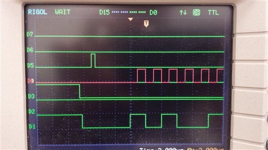
    As you can see, all 8 bits for 0xA5 are transmitted, but after 8 data transfers.  What also puzzles me is why would the RX interrupt occur at the beginning of the data transfer.  I've posted a picture of it below.  Please let me know what you think of this.

  • I don’t see you selecting the slave. Usually, you have a chip select signal for selecting the slave. (one dedicated GPIO pin for each slave). Before starting a transfer, you pull it low, and after the transfer is done (which is NOT the moment when you write the last byte to TXBUF) you pull it high again.
    This job is NOT done by the STE pin. STE is a plain input in slave or multi-master mode and without any use in single master mode.

    Next thing is that your while loop writes to TXBUF as long as no transmit interrupt is pending. So as soon as the USCI is ready to receive a byte, you stop pushing bytes into TXBUF (which is good, as you have an ISR to handle this), and in the meantime, you flood it with bytes even though it is not ready to take them.

     After clearing SWRST, you clear TXIFG. It won’t come back until the next byte has been sent. That’s okay if (and only if) the rest of the code is doing things properly.

    The way to go is:

    Init the USCI
    clear TXIFG
    set TXIE
    fill an array with data
    set-up the ISR to transfer form the second (!) byte on
    write the first byte to TXBUF.
    When the ISR has read the last byte, it clears TXIFG or even TXIE.

     One final note: You don’t write what your scope signals are. But I guess, the red one is the SPI clock, while D5 is your strobe? I don’t see 8 transfers on the screenshot. I see the first 6 clock cycles of the first transfer, transmitting the first 6 bits. And MISO is 0xFF because after these 6 clock cycles, nothing has been received yet form the slave. Of course the slave can only answer once it has received the first byte - unless it is constantly sending a status byte. But if the slave isn’t selected, it will most likely not send anything at all.

  • Jens-Michael Gross said:
    I don’t see you selecting the slave.

    The STE pin is controlled by the master, and the master pulls the pin low when it wants to be active.  Since the MSP430 is acting like a slave device, I'm aware that the slave won't have any control over this pin.

    Jens-Michael Gross said:
    Next thing is that your while loop writes to TXBUF as long as no transmit interrupt is pending. So as soon as the USCI is ready to receive a byte, you stop pushing bytes into TXBUF (which is good, as you have an ISR to handle this), and in the meantime, you flood it with bytes even though it is not ready to take them.

    That does make sense.  I've changed the main code so that it does the following:

    /*
     * main.c
     */
    int main(void) {
        //WDTCTL = WDTPW | WDTHOLD;	// Stop watchdog timer in SYSTEM_init() function
    	SYSTEM_init();
    	while (1)
    	{
    		if (!(UCA0IFG&UCRXIFG)) //If no transmit interrupt pending.
    		{
    			UCA0IFG |= UCTXIFG; // Set the TXIFG so that an interrupt is pending
    		}
    }
    
    		//else UCA0TXBUF = 0xA5;
    	}
    

    Unfortunately, the same issue occurs when I updated my code.

    Jens-Michael Gross said:
    One final note: You don’t write what your scope signals are.

    Oops.  I'll list what scope signals are from the top of the image downwards:

    • D6: STROBE2
    • D5: STROBE1
    • D0: SCLK
    • D3: STE (or slave select)
    • D2: MISO
    • D1: MOSI

    Jens-Michael Gross said:
    I don’t see 8 transfers on the screenshot. I see the first 6 clock cycles of the first transfer, transmitting the first 6 bits.

    I should have explained this a little better.  What I should expect happen is that after a transfer occurs (lasting 8 clock cycles), the MSP430 should send the byte 0xA5, bit by bit along each clock cycle.  What is happening instead is that the the byte 0xA5 is being transferred, bit by bit along each transmission. That means that after the transmission is over, the MISO changes its bit.  Then, after the eighth transfer, the RX interrupt occurs. 

    One thought was that the SPI clock speed of 500kHz would have caused it.  However, I concluded that it wasn't the case, since I saw the same issue occur when the SPI clock was at 7kHz.

  • You know that STE is just controlling the input driver of SCLK and the output driver of MISO. It does not, by any means, do anything to the USCI state machine. Think of STE like a relay control that connects and disconnects the clock in and data out lines. Not more. So during master port pin initialization, the slave may already pick-up signals and misinterpret them.
    If you are the only slave, using STE is totally superfluous and won’t give you any benefit.
    But you should catch the chip select form the master by a port pin with interrupt, and when received, clear SWRST and write your first byte to TXBUF. And when CS is released, put the USCI back in reset (an consider the communication done).

    Regarding your screenshot, are you sure you didn’t twist the signals? D1 looks like the beginning (first 6 bit) of 0xA5. Which would fit the slave output. But according to your legend, it is the master output.
    Also, an RX interrupt makes no sense without a previous transfer., However, right after SWRST is cleared, a TX interrupt is generated (to fill the then empty TXBUF).
    Another idea: if you get one bit sent on each transfer (of 8 clock cycles), you maybe wired CS to the clock input? This would be a possible explanation why you only see one bit send on each transfer - each transfer generates one clock pulse on the clock input by the CS signal and the clock signal goes into the void.

    BTW: by the large width of the short strobe pulse compared to the clock width, you can see that you SPI clock is quite high, in relation to your MCLK speed. Until you got it running, you might want to lower the SPI speed, or the transfers might be faster than your code can react.

    Finally, are you sure of the correct SPI mode? The most common one ha UCPL set and UCPH clear. The notation on the MSP is different from the Motorola notation, so you need to check the meaning of the signals, not the mode nr or the bit value.

  • Jens-Michael Gross said:
    If you are the only slave, using STE is totally superfluous and won’t give you any benefit.

    Good point! I've changed the configuration of the code so that it runs as a "3-pin SPI".  However, there was no change to the functionality of the code in this configuration.

    Jens-Michael Gross said:
    But you should catch the chip select form the master by a port pin with interrupt, and when received, clear SWRST and write your first byte to TXBUF. And when CS is released, put the USCI back in reset (an consider the communication done).

    I did try this.  Below is how I configured the GPIO pins to reflect this:

    	P1IES &= ~BIT4;                           // P1.4 Lo/Hi edge, so that the interrupt occurs after the transmission
    	P1IE = BIT4;                              // P1.4 interrupt enabled
    	P1IFG &= ~BIT4;                           // P1.4 IFG cleared

    Then, I added this ISR below.

    // Port 1 interrupt service routine
    // Resets the SPI just in case
    #pragma vector=PORT1_VECTOR
    __interrupt void Port_1(void)
    {
    	UCA0TXBUF = 0xA5;
    	UCA0CTL1 |= UCSWRST;
    	UCA0CTL1 &= ~UCSWRST;
    	UCA0IE |= UCTXIE;
    	P1IFG &= ~BIT4;                         // Clear P1.4 IFG
    	P1IE = 0;
    	__bic_SR_register_on_exit(CPUOFF);// Wake up to setup next TX
    
    }

    This addition didn't change the functionality of my code.  I also checked to see if this ISR would ever occur, and it didn't.

    Jens-Michael Gross said:
    Regarding your screenshot, are you sure you didn’t twist the signals? D1 looks like the beginning (first 6 bit) of 0xA5. Which would fit the slave output. But according to your legend, it is the master output.

    I'll get another picture of the oscilloscope that shows the SPI Master transmitting a different signal to show proof.  But in short, the D1 signal is the MOSI pin.

    Jens-Michael Gross said:
    BTW: by the large width of the short strobe pulse compared to the clock width, you can see that you SPI clock is quite high, in relation to your MCLK speed. Until you got it running, you might want to lower the SPI speed, or the transfers might be faster than your code can react.

    Another good point.  I did actually change the SPI master so that the SPI Clock is running at 7kHz.

    Jens-Michael Gross said:
    Finally, are you sure of the correct SPI mode? The most common one ha UCPL set and UCPH clear. The notation on the MSP is different from the Motorola notation, so you need to check the meaning of the signals, not the mode nr or the bit value.

    I did try all the possible modes that could work with this, and the code still doesn't run differently. 

    Jens-Michael Gross said:
    Another idea: if you get one bit sent on each transfer (of 8 clock cycles), you maybe wired CS to the clock input? This would be a possible explanation why you only see one bit send on each transfer - each transfer generates one clock pulse on the clock input by the CS signal and the clock signal goes into the void.

    That was definitely my first reaction with seeing what was happening.  I've checked again, and yes, the CS and the SCLK pins are connected appropriately.

    What I am confused about is in the case that I instruct the SPI Master (Raspberry Pi) to send two bytes at a time (sending two 8-bit bytes, requiring 16 clock cycles).  What I should ideally see is that after the first byte, the MSP430 should get into the SPI RX ISR.  Instead, I see one bit sent on each two transfer (16 clock cycles).  Again, I would think that the SCLK and CS pins are swapped, but I've checked it again and again. 


    What I've also tried is to run the example SPI Slave echo code Code Composer Studio offers, and that doesn't work either.  I'm really unsure what else to try at this point.  I'll keep thinking of possible solutions.

  • The port ISR looks suspicious. You configure the interrupt to trigger at the rising edge (after transmission, CS de-asserted). However, inside the ISR, you set and clear SWRST, which will discard the just received incoming data (if not already read) and set TXIFG. SO when you now return from the port ISR, the TX ISR is called immediately, before the main code (which you wake with clearing CPUOFF on exit) has a chance to do anything.
    After the transfer, disable the USCI interrupts, wake main, and let main set-up the USCI for the next transfer and enable interrupts again when ready.

  • Jens-Michael Gross said:
    The port ISR looks suspicious

    The problem here is that the Port ISR is not responding at all.  I get what you are saying that the TXIFG shouldn't be set inside to avoid the main code from doing anything. But if I try to toggle a strobe pin in here, wouldn't I see it come up at last once?  Either way, I've changed this in my code, and the iSR still doesn't work properly, or any differently from before.

    Jens-Michael Gross said:
    After the transfer, disable the USCI interrupts, wake main, and let main set-up the USCI for the next transfer and enable interrupts again when ready.

    I get how to disable the interrupts inside the ISR, but I'm not sure if I get the statement "wake main".  I know that the program continues off where it left off after the ISR is done.  I'm not sure whether or not it starts at the beginning, and if not, will I have to create a loop to reconfigure the SPI after it returns from the ISR.

    This all seems odd, to be honest. I've tried using the sample code with no luck.  I've even brought back a previous project I worked with using the FR5739 and SPI module with the same problem.  The iSR refuses to work properly, and the SPI module refuses to transmit. 

    Would it be possible if it was something to so with the hardware?  I've verified that everything is connected properly (again and again), but I still can't explain why this would not work. 

  • With ‘wake main’, I meant:

    Your main code enters LPM. At this point, execution of main stops, as the CPU doesn’t get any clock pulse except when entering an ISR. When the port pin ISR is called, it ends LPM by clearing OSCOFF on exit. This would make main continuing past the __bis_SR_register(LPM0_bits|GIE) statement (well, in your first post, this line was commented and replaced by just enabling interrupts). Now main would know that the chip select came, and could prepare the USCI for the transmission.
    Of course, this can also be done in the port pin ISR. However, as soon as SWRST is cleared, TXIFG is pending and when the port ISR exits, the USCI ISR is immediately called and main has no chance to do anything.
    For fastest reaction time, there is also the possibility to directly stuff TXBUF inside the port pin ISR right after clearing SWRST. This would give the shortest delay between chip select and being ready for the transfer.


    Nevertheless, the port pin ISR should trigger and if you have a pin toggle in it, it should toggle. Except if a higher-priority interrupt is pending and looping all the time, which would prevent main or any other lower-priority interrupt to execute.

    Since you say that even the demo code isn’t working, It might indeed be a hardware problem too. The MSPs are real die-hards but of course they can be destroyed. Completely or individual pins. So what about signal levels? Does the master send 5V TTL signals while the MSP has 3.3V VCC? This would kill the port pins.

    Also, are you sure that your code is executing at all? Or is it running in a simulator? (in this case, you could step through the code as if it were executing on the real chip, but of course no external events will trigger an interrupt and no output signals will appear on the real MSP). Happened a lot on older versions of IAR when people misconfigured the IDE, selecting ‘simulator’ instead of ‘emulator’.

**Attention** This is a public forum