This thread has been locked.

If you have a related question, please click the "Ask a related question" button in the top right corner. The newly created question will be automatically linked to this question.

Clipped sine wave into XT2 input on the MSP4305529

Other Parts Discussed in Thread: MSP430F149, MSP430F5529

The previous generation of products at my company use an MSP430F149 with a 1Vp-p clipped sine wave TCXO connected directly to the XT2 input. We have tried the same thing with the MSP430F5529 and it appears to be working when the XT2 input set enabled to expect and external crystal (not in bypass mode). Is it acceptable to drive the XT2 input in this way with a 1 Vp-p clipped sine wave input? Does it need to be AC-coupled or is there internal AC coupling? It appears to be working on the first prototype unit but I'm concerned that it may not meet spec and won't operate correctly in production or the field.

Thanks!

Charlie

  • Is your sine wave 1Vpp going down to negative voltages? What is your supply voltage? Does the signal meet the requirements concerning the amplitude mentioned on page 33 in the datasheet?
  • Thanks for your help Dennis.

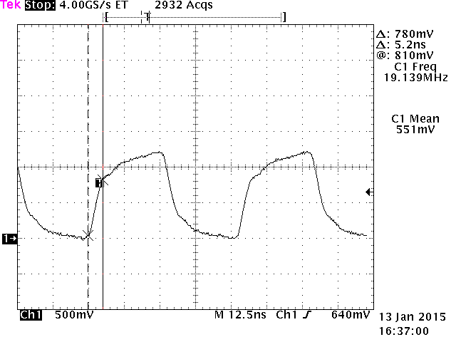
    The signal is 1Vpp, but does not go negative.  It is DC coupled (routed directly from the TCXO to the MSP430) and is 0-1V.  Both the TCXO and the MSP430 are running at 3.3V.  Page 33 of the MSP430F5529 datasheet does not have any amplitude requirements.  Page 59 describes the specifications for the XT2 input in oscillator mode, which is the mode we're using, but it does not provide voltage parameters for the input signal.  Voltage parameters are provided for bypass mode (not using this mode) on page 54 (same as the Schmitt Trigger inputs) which are not met.  The TCXO input works in external crystal mode, but not in bypass mode.

    Here's a scope capture of the TCXO output.

    Thanks again!

  • My fault - page 33 was the datasheet of the F149 :-\

    In the datasheet for the F5529 I cannot see that information, too.

    Maybe somebody more experienced can answer your question - sorry! I'm out here.

    Dennis

  • In oscillator mode, the clock signal is taken from the XOUT pin, the output of the inverter gate of the pierce oscillator circuit. So if you attach a sine signal to XIN, it goes through the inverter as signal conditioner. In bypass mode, the input signal is directly taken as digital input signal form the XIN pin, so it must be a proper digital signal, matching the input thresholds and duty cycle.
    In your case, if you attach a crystal like signal to XIN in oscillator mode, the inverter will output the signal to XOUT and this is taken for the clock input. It is not necessary that XOUT is connected to a crystal to cause the oscillation or is left open externally.
    For XTAL pins that are not shared with port pins, the datasheets do not contain schematics, but I guess it is done the same way.
  • Thanks Jens-Michael, That makes sense. We have contacted a TI FAE and are waiting his reply. I'll check back in with the solution, if there is one.

    Thanks again!

    -Charlie

**Attention** This is a public forum