This thread has been locked.

If you have a related question, please click the "Ask a related question" button in the top right corner. The newly created question will be automatically linked to this question.

Add Delay to PWM code in MSP430FR5969

Other Parts Discussed in Thread: MSP430FR5969

I have a code that generates a PWM. Can someone tell me how to add code to the existing to generate a PWM and give it a delay to certain amount and get that out through one of the ports?

  • Yashaswy,

    please provide some more information. Which code do you refer to? And I do not understand your "delay" - what are you planning to do? Please give a more detailed explanation about this.

    Dennis
  • I have the example PWM code. I want to generate pulses like the one in the code. So I want to generate two pulses which are at a delay to each other. How do I generate both the pulses?
  • Since you still did not mention your code example, here a basic approach:

    Use a timer in continuous mode. Set any output pin high and start the timer. In the ISR, set the output pin low and add the off time to the CCRx register. In the next interrupt, set the pin high and add the high time to CCRx. The next interrupt, set the pin low again and stop the timer. You got two pulses.
  • This is the code....
    MSP430FR59x Demo - Timer1_A3, PWM TA1.1-2, Up Mode, DCO SMCLK
    Can you help now to get multiple pulses out of these
  • What have you tried so far? Please upload the code with your changes so there is something to discuss.
  • I've run this code....

    msp430fr59xx_ta0_16

    the output from P1.2 has 75% data cycle
    and output from P1.3 has 25% data cycle...

    Now I want to give the output from P1.3 an offset.. How do I give that?
  • Did you have a look into the user's guide of the processor already? It isn't too bad to read the chapter about the timer first - this gives you a basic understanding of it's working principle and the different modes.
  • Yes, but how do I show it in the code?
  • Also we need two timers to do that. We have that in msp430
  • Yashaswy,

    when you heave read the user's guide, then why not try my first comment with the timer in continuous mode. To be honest: I still don't know what you want to do. Is it a repeated two pulse burst, or only once? How long are the pulses and the pauses in between? Why not try something yourself first?

    Dennis
  • Dennis,
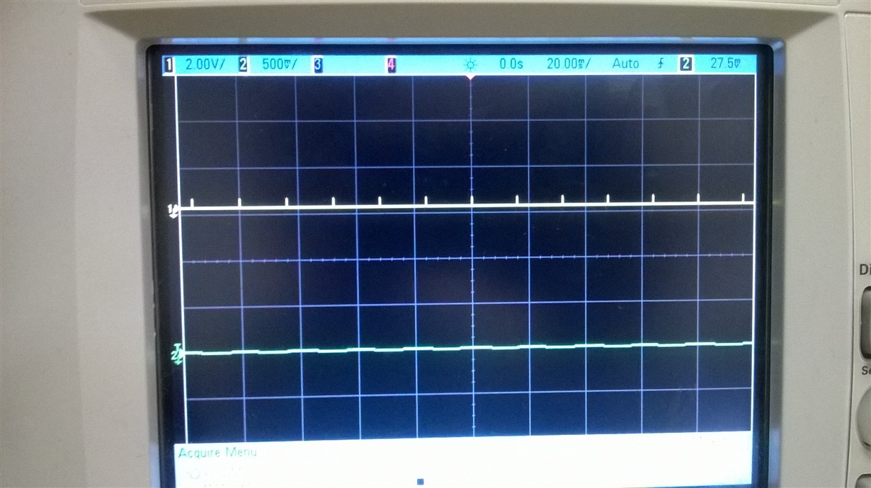
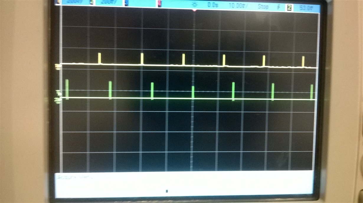
    I have tried changing the code and I'm getting pulses. The two pulses coming out in 2 channels (both with T-on as 200us and Time period as 20ms ) are seen in the oscilloscope I have. I want to given both of them a delay of say 10ms... how do I do that is what I'm asking
  • That sounds good! Can you upload your code please?
  • This is the code

    #include <msp430.h>

    int main(void)
    {
    WDTCTL = WDTPW | WDTHOLD; // Stop WDT

    // Configure GPIO
    P1DIR |= BIT2 | BIT3; // P1.2 and P1.3 output
    P1SEL0 |= BIT2 | BIT3; // P1.2 and P1.3 options select

    // Disable the GPIO power-on default high-impedance mode to activate
    // previously configured port settings
    PM5CTL0 &= ~LOCKLPM5;

    CSCTL0_H = CSKEY >> 8; // Unlock CS registers
    CSCTL1 = DCOFSEL_6; // Set DCO to 8MHz
    CSCTL2 = SELA__VLOCLK | SELS__DCOCLK | SELM__DCOCLK;// Set ACLK = VLO; SMCLK = DCO/8
    CSCTL3 = DIVA__8 | DIVS__8 | DIVM__8; // Set all dividers
    CSCTL0_H = 0;

    TA1CCR0 = 20000-1; // PWM Period
    TA1CCTL1 = OUTMOD_7; // CCR1 reset/set
    TA1CCR1 = 200; // CCR1 PWM duty cycle
    TA1CCTL2 = OUTMOD_7; // CCR2 reset/set
    TA1CCR2 = 200; // CCR2 PWM duty cycle
    TA1CTL = TASSEL__SMCLK | MC__UP | TACLR; // SMCLK, up mode, clear TAR

    __bis_SR_register(LPM0_bits); // Enter LPM0
    __no_operation(); // For debugger
    }
  • So one of them gets a delay of 10ms. How do we do it?
  • A delay to what? Yashaswy, please describe in detail the waveform(s) you expect from your program! The hardware PWM only might not do the job for that since it's felixibility is limited. You will have to work with the interrupts of the timer.

    It sounds like you want to do something like in this thread:

    Maybe you review this question. If you want to do something similar, then you can build your code around the given example there.

    Dennis

  • I want the EXACT output out of the MSP430FR5969 controller. Can you help me by modifying the code I submitted above?
  • Yashaswy,

    sorry, but we will not find a solution for you if you do not clearly specify what you are expecting.

    Yashaswy Akella said:
    I want the EXACT output

    What does that mean? I asked multiple times now to get an idea of what you want. I know that you want two (PWM) pulses with a delay, but that is all so far. I posted a link to a similar example program, but you did not say anything regarding my suggestion, so still no one knows your plans. If you want help with your program you will have to povide some more information and you will have to invest some of your own energy and time. Maybe you have a short look at this article:

    Especially 3) and 4)

    Dennis

  • Dennis,
    I've done some homework on this and understood that there are 5 timers on MSP430FR5969, out of which we will be using Timer A 0 and Timer A 1 for I/O ports P1.2, P1.3 respectively. I've flashed this code but only the output from P1.2 is coming. Can you check it and correct it?

    Thanks a lot!!


    #include <msp430.h>

    int main(void)
    {

    WDTCTL = WDTPW | WDTHOLD; // Stop WDT

    // Configure GPIO
    P1DIR |= BIT2 | BIT3;
    P1SEL0 |= BIT2 |BIT3;

    PM5CTL0 &= ~LOCKLPM5;

    CSCTL0_H = CSKEY >> 8; // Unlock CS registers
    CSCTL1 = DCOFSEL_6; // Set DCO = 8MHz
    CSCTL2 = SELA__VLOCLK | SELS__DCOCLK | SELM__DCOCLK;// Set ACLK=VLO SMCLK=DCO
    CSCTL3 = DIVA__8 | DIVS__8 | DIVM__8; // Set all dividers
    CSCTL0_H = 0; // Lock CS registers

    // Configure Timer0_A
    TA0CCR0 = 16000-1;
    TA0CCR1 = 20;
    TA0CCR2 = 12000-1;
    TA0CCTL1 = OUTMOD_7;
    TA0CCTL2 = CCIE;
    TA0CTL = TASSEL_2 | ID_0 | MC_1 | TACLR;


    TA1CCR0 = 16000-1;
    TA1CCR1 = 20;
    TA1CCTL1 = OUTMOD_7;


    TA1CTL = TASSEL__SMCLK | MC__UP | TACLR; // SMCLK, up mode, clear TAR


    __bis_SR_register(LPM0_bits); // Enter LPM0
    __no_operation(); // For debugger
    while (1);
    }


    #pragma vector = TIMER0_A1_VECTOR // Compare interrupt for 25% elapsed duty cycle
    __interrupt void TIMER0_A1_ISR( void )
    {
    TA1CTL = TASSEL_2 | ID_0 | MC_1 | TACLR; // 2nd PWM: SMCLK, divider 1, up-mode, clear
    TA0CCTL2 = 0x00; // Clear compare interrupt - executed only once
    }
  • Yashaswy Akella said:
    ... we will be using Timer A 0 and Timer A 1 for I/O ports P1.2, P1.3 respectively...

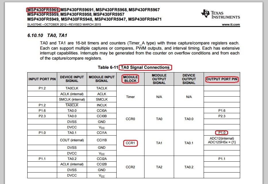
    P1.2 cannot be used as PWM output for TA0. Only P1.6/P2.3, P1.0, or P1.1 can be used.

    P1.3 is okay for PWM output of TA1. So is P1.2

    Yashaswy Akella said:
    ... I've flashed this code...

    You couldn't have flashed any code. You have framed the code ;)

    Yashaswy Akella said:
    ... but only the output from P1.2 is coming...

    That is because the code is incorrect for your purpose. You started the entire thread talking about the code. It turns out to be the wrong code.

  • Yashaswy Akella said:
    #pragma vector = TIMER0_A1_VECTOR // Compare interrupt for 25% elapsed duty cycle
    __interrupt void TIMER0_A1_ISR( void )
    {
       TA1CTL = TASSEL_2 | ID_0 | MC_1 | TACLR; // 2nd PWM: SMCLK, divider 1, up-mode, clear
       TA0CCTL2 = 0x00; // Clear compare interrupt - executed only once
    }

    Your interrupt will not be executed because you did not enable the global interrupts.

  • Hey old_cow_yellow,
    I've worked on the code and flashed it but it did not work. Agree that I framed it but that was because I'm not too good in programming.
    Any sample code by TI for MSP430FR5969 on this concept will actually teach me how to go ahead. Can you help me? Please :)

    Regards,
    Yashaswy
  • Dennis,
    The last part in the code was taken from the example you gave me above in this thread.

    Regards,
    Yashaswy
  • Yashaswy Akella said:
    The last part in the code was taken from the example you gave me above in this thread.

    Yes, I saw that, but in my code I did:

    __bis_SR_register( GIE ); // Enable interrupts

    Simply add the GIE enable in your code.

    Dennis

  • That was added in the above loop right!
    Do I need to add in again in this loop?
  • Hey OCY,
    If P1.6 and P2.3 are both same then tell me how to check the outputs in the registers for this example
    e2e.ti.com/.../1607730

    Also tell me which timers are restricted to which of the I/O ports

    Regards,
    Yashaswy
  • This kind of information can always be found in the respective Data-Sheets of the chips.
  • Dear OCY,
    I've made the changes and flashed the code again. Only the output from P1.2 is coming. I've checked the code but there is no output from P1.6
    Please tell me what's wrong in here.


    #include <msp430.h>

    int main(void)
    {

    WDTCTL = WDTPW | WDTHOLD; // Stop WDT

    // Configure GPIO
    P1DIR = BIT6;
    P1SEL0 = BIT6;

    P1DIR = BIT2;
    P1SEL0= BIT2;

    PM5CTL0 &= ~LOCKLPM5;

    CSCTL0_H = CSKEY >> 8; // Unlock CS registers
    CSCTL1 = DCOFSEL_6; // Set DCO = 8MHz
    CSCTL2 = SELA__VLOCLK | SELS__DCOCLK | SELM__DCOCLK;// Set ACLK=VLO SMCLK=DCO
    CSCTL3 = DIVA__8 | DIVS__8 | DIVM__8; // Set all dividers
    CSCTL0_H = 0; // Lock CS registers

    // Configure Timer0_A
    TA0CCR0 = 16000-1;
    TA0CCR1 = 20;
    TA0CCR2 = 12000-1;
    TA0CCTL1 = OUTMOD_7;
    TA0CCTL2 = CCIE;
    TA0CTL = TASSEL_2 | ID_0 | MC_1 | TACLR;


    TA1CCR0 = 16000-1;
    TA1CCR1 = 20;
    TA1CCTL1 = OUTMOD_7;


    TA1CTL = TASSEL__SMCLK | MC__UP | TACLR;


    __bis_SR_register(GIE); // Enter LPM0
    __no_operation(); // For debugger
    while (1);
    }


    #pragma vector = TIMER0_A1_VECTOR
    __interrupt void TIMER0_A1_ISR( void )
    {
    TA1CTL = TASSEL_2 | ID_0 | MC_1 | TACLR;
    TA0CCTL2 = 0x00;
    }
  • Your code for TA0 is generating PWM output at CCR1.

    Yashaswy Akella said:
    // Configure Timer0_A
    TA0CCR0 = 16000-1;
    TA0CCR1 = 20;
    TA0CCR2 = 12000-1;
    TA0CCTL1 = OUTMOD_7;
    TA0CCTL2 = CCIE;
    TA0CTL = TASSEL_2 | ID_0 | MC_1 | TACLR;

    According to the Data-Sheet PWM output from CCR1 can only go to P1.0. 

  • One more doubt. Cant I use both P1.2 and P1.3 from T A 1 and get a delay between them?
    because the ports 1.6/2.3, P1.0, P1.1 are not accessible to get the output from hardware
  • // Configure Timer0_A
    TA0CCR0 = 16000-1;
    TA0CCR0 = 20;
    TA0CCR1 = 12000-1;
    TA0CCTL1 = OUTMOD_7;
    TA0CCTL2 = CCIE;
    TA0CTL = TASSEL_2 | ID_0 | MC_1 | TACLR;

    I changed only this part in the entire code as per your suggestion but there is not output from P1.6
  • P1.2 and P1.3 can be used for PWM signals generated by TA1 CCR1 and CCR2 respectively. They can have different pulse lengths, but will always either start at the same time, or end at the same time. (I think you have already tried this.)

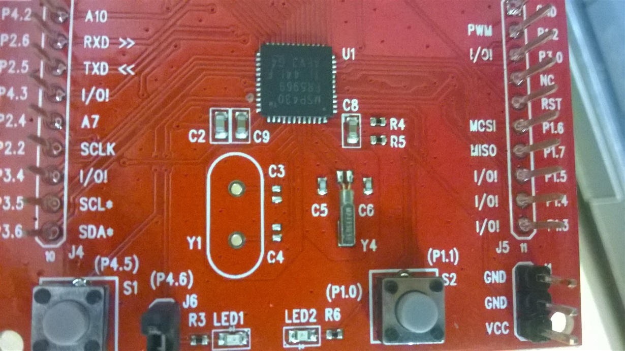
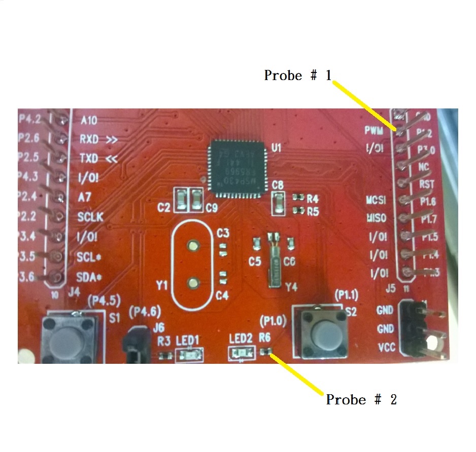
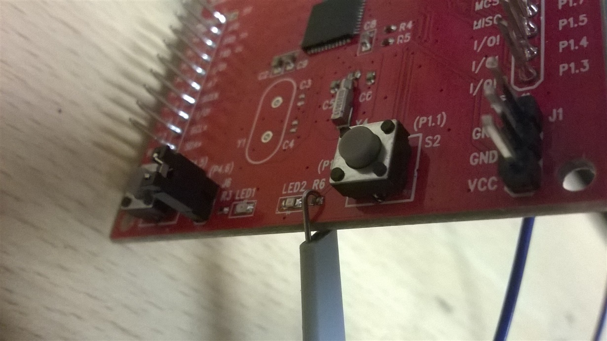
    If you are just using a scope probe to verify the signals, P1.0 is accessible at the right-hand end of R6 next to LED2.
  • Yes, I've tried that P1.2 and P1.3 thing. The P1.0 is not a port right. It's a switch in my controller

  • No, P1.1 is the switch. As OCY said: "...right-hand end of R6 next to LED2" - P1.0 is connected to the LED.
  • So how to get the output out of the switch?
    I mean which port to connect as there is nothing behind the switch
  • Yashaswy Akella said:
    So how to get the output out of the switch?

    Output of the switch?

    The pin the switch is connected to should be configured as an input. Of course you can use it as an output, but then you should not press the switch because...

    Yashaswy Akella said:
    I mean which port to connect as there is nothing behind the switch

    ..."behind the switch" is GND - you would short the pin.

  • This is what I understood - that P1.1 must be given as input to some other port like P1.7 so that we can actually get the output from the port to see that in hardware. Right?
  • Sorry, I shouldn't have said that. I will try to explain in a few minuets.
  • Yashaswy Akella wrote the following post at Sun, Nov 8 2015 10:25 PM:

    Yashaswy Akella said:
    // Configure Timer0_A
    TA0CCR0 = 16000-1;
    TA0CCR0 = 20;
    TA0CCR1 = 12000-1;
    TA0CCTL1 = OUTMOD_7;
    TA0CCTL2 = CCIE;
    TA0CTL = TASSEL_2 | ID_0 | MC_1 | TACLR;

    I changed only this part in the entire code as per your suggestion but there is not output from P1.6

    1. You first set TA0CCR0 to 10000-1, but then immediately change it to 20. And TA0CCR1 is set to 12000-1, which is larger than 20. This does not make any sense.
    2. This entire exercise has nothing to do with what I said.
  • Sun, Nov 8 2015 10:33 PM, old_cow_yellow:

    P1.0 is accessible at the right-hand end of R6 next to LED2.


    Sun, Nov 8 2015 10:46 PM Yashaswy Akella:

    The P1.0 is not a port right. It's a switch in my controller.


    Sun, Nov 8 2015 11:27 PM Dennis Eichmann:

    No, P1.1 is the switch. As OCY said: "...right-hand end of R6 next to LED2" - P1.0 is connected to the LED.


    Sun, Nov 8 2015 11:34 PM Yashaswy Akella:

    So how to get the output out of the switch?

    I mean which port to connect as there 

    P1.0 is not a switch

  • Oh sorry, now I get it OCY. As Dennis said that we can send the output from P1.0 internally to another hardware port where we can connect the probe of our oscilloscope, I actually liked the idea. Can you tell me how to do it. Also please check the message I sent you. Thank you.

    Regards,
    Yashaswy
  • Honestly I still don't know what you are planning to do - maybe it is just me, but I don't get it. I read the complete thread again and still cannot figure out what your program shall do in the end.

  • I thought I was too old. But you are cool!
  • #include <msp430.h>

    int main(void)

    {

    WDTCTL = WDTPW | WDTHOLD; // Stop WDT

    // Configure GPIO

    P1DIR = BIT6 BIT0;

    P1SEL0 = BIT6 BIT0;

    P1DIR = BIT2;

    P1SEL0= BIT2;

    PM5CTL0 &= ~LOCKLPM5;

    CSCTL0_H = CSKEY >> 8; // Unlock CS registers

    CSCTL1 = DCOFSEL_6; // Set DCO = 8MHz

    CSCTL2 = SELA__VLOCLK | SELS__DCOCLK | SELM__DCOCLK;// Set ACLK=VLO SMCLK=DCO

    CSCTL3 = DIVA__8 | DIVS__8 | DIVM__8; // Set all dividers

    CSCTL0_H = 0; // Lock CS registers

    // Configure Timer0_A

    TA0CCR0 = 16000-1;

    TA0CCR1 = 20;

    TA0CCR2 = 12000-1;

    TA0CCTL1 = OUTMOD_7;

    TA0CCTL2 = CCIE;

    TA0CTL = TASSEL_2 | ID_0 | MC_1 | TACLR;

    TA1CCR0 = 16000-1;

    TA1CCR1 = 20;

    TA1CCTL1 = OUTMOD_7;

    TA1CTL = TASSEL__SMCLK | MC__UP | TACLR;

    __bis_SR_register(GIE); // Enter LPM0

    __no_operation(); // For debugger

    while (1);

    }

    #pragma vector = TIMER0_A1_VECTOR

    __interrupt void TIMER0_A1_ISR( void )

    {

    TA1CTL = TASSEL_2 | ID_0 | MC_1 | TACLR;

    TA0CCTL2 = 0x00;

    }


  • Dennis, 

    The code I need will create Two pulses with Time period 16ms each with one being ahead of another by 12ms(which is delay) in an MSP430FR5969 controller.

    Regards,

    Yashaswy

  • OCY,

    Thank you for investing time and helping me code this but it is not giving the output out of P1.0. Am I doing it the right way? because, I'm getting the output out of P1.2 but not from P1.0 . Please help

    Regards,

    Yashaswy

  • The source code had some mistakes that I did not see. They are corrected as follows:

    #include <msp430.h>
    
    int main(void)
    {
      WDTCTL = WDTPW | WDTHOLD; // Stop WDT
      // Cofigure GPIO
      P1DIR = BIT2 | BIT0;
      P1SEL0 = BIT2 | BIT0;
      PM5CTL0 &= ~LOCKLPM5;
      CSCTL0_H = CSKEY >> 8; // Unlock CS registers
      CSCTL1 = DCOFSEL_6; // Set DCO = 8MHz
      CSCTL2 = SELA__VLOCLK | SELS__DCOCLK | SELM__DCOCLK;// Set ACLK=VLO SMCLK=DCO
      CSCTL3 = DIVA__8 | DIVS__8 | DIVM__8; // Set all dividers
      CSCTL0_H = 0; // Lock CS registers
      // Configure Timer0_A
      TA0CCR0 = 16000-1;
      TA0CCR1 = 20;
      TA0CCR2 = 12000-1;
      TA0CCTL1 = OUTMOD_7;
      TA0CCTL2 = CCIE;
      TA0CTL = TASSEL_2 | ID_0 | MC_1 | TACLR;
      TA1CCR0 = 16000-1;
      TA1CCR1 = 20;
      TA1CCTL1 = OUTMOD_7;
      __bis_SR_register(GIE); // Enter LPM0
      __no_operation(); // For debugger
      while (1);
    }
    
    #pragma vector = TIMER0_A1_VECTOR
    __interrupt void TIMER0_A1_ISR( void )
    {
      TA1CTL = TASSEL_2 | ID_0 | MC_1 | TACLR;
      TA0CCTL2 = 0x00;
    }

  • OCY,

    You are amazing!! Thank you for helping me out.

    I wanted this and I'm getting it. I'll get back if I have any more queries :)

**Attention** This is a public forum