This thread has been locked.

If you have a related question, please click the "Ask a related question" button in the top right corner. The newly created question will be automatically linked to this question.

SPI - MSP430F2274 with ADXL345

Other Parts Discussed in Thread: MSP430F2274, CC2500, MSP430F2132, MSP430F5438A, MSP430G2553

Hello everyone,

I am a newbie to MSP430 and SPI protocol. I read a lot about SPI online and also in the User Guide of MCU. The problem I am facing is described below;

I am interfacing ADXL345 Accelerometer with MSP430F2274 via  3 wire SPI. I think I am doing all the initializing correctly, but I am not getting any useful data back.

I am trying to read the device ID of ADXL345 but I keep on getting 0xF2 instead of 0xE5. 

This is the data sheet for ADXL345; http://www.analog.com/static/imported-files/data_sheets/ADXL345.pdf

ADXL345 takes 16 bits of data at one time but the MCU can only clock out 8 bits in one transmission, I think this creates a timing difference in the communication and hence

I don’t get what I want. Below is the code I am trying to use:

#include "msp430x22x4.h"

volatile unsigned char Data;
volatile int i;
void main(void)
{
  WDTCTL = WDTPW + WDTHOLD;                                           // Stop watchdog timer
  P3SEL |= 0x31;                                                                             // P3.0,P3.4,P3.5 USCI_A0 option select
  P3DIR |= 0x40;                                                                             // P3.6 output direction
  P4DIR |= BIT3;                                                                             // Used to provide power to the Accelerometer 
  P4OUT &= ~BIT3;     
   

                                      // SPI initialization 
  UCA0CTL0 |= UCCKPH + UCCKPL + UCMSB + UCMST + UCSYNC;              // 3-pin, 8-bit SPI master
  UCA0CTL1 |= UCSSEL_2;                                                       // Select SMCLK as CLK
  UCA0BR0 |= 0x02;
  UCA0BR1 = 0;                             
  UCA0MCTL = 0;
  UCA0CTL1 &= ~UCSWRST;                                                   // **Initialize USCI state machine**
  P4OUT |= BIT3;                                                                          // Turn the Accelerometer on
  while(1)
  {
 
    P3OUT  &= ~0x40;                                                                           // Chip select active low
    for(i = 0xFFFF; i > 0; i--);                                                             // Delay
    IFG2 &= ~UCA0RXIFG;                                                              // Clear int flag
    while ((IFG2 & UCA0TXIFG) == 0);
    UCA0TXBUF = 0xC0;                                                               // Read Dev ID
    IFG2 &= ~UCA0RXIFG;
    //while ((IFG2 & UCA0TXIFG) == 0);                                     // TXBUF ready?                    
    UCA0TXBUF = 0x45;
    while ((IFG2 & UCA0TXIFG) == 0);                                      // TXBUF ready?  
    P3OUT |= 0x40;                                                                      // End Transmission
    while ((IFG2 & UCA0RXIFG) == 0);                                       // RXBUF ready?
    Data = UCA0RXBUF;                                                               // Move value
  
  }
}

Somebody please help me on this.

Thanks.

  • Just now I successfully  read the Device Id.

  • Satbir Sekhon said:
    I keep on getting 0xF2 instead of 0xE5

    So what you expect is
    11100101
    and what you get is
    11110010

    Looks like you're getting a superfluous '1' as the first bit and miss the last. This may be caused by a wrong clock edge setting. Or because the time between setting the chip select low and clocking the first byte is too short, so the first clock pulse is ignored.

    Satbir Sekhon said:
       for(i = 0xFFFF; i > 0; i--);                                                             // Delay


    This is no delay. This is dead code and (hopefully) optimized away by the compiler.
    All it does is setting i to 0. Making it volatile most likely won't help here.
    For delays of any sort, either use a timer (this is the exact way and behaves identically even on differently clocked systems) or use the __delay_cycles() intrinsic, which will change the outcome depending on the current MCLK frequency, but at least won't be optimized. And as the very last option, add a __no_operation() into the for loop. This will force the compiler to not consider the loop as dead code. It might, however, partially unroll the loop, so the delay time might change depending on the compiler type and revision and optimization level.

    Also, don't deselect CS before the last byte has been received. The slave might immediately stop sending and you'll get only half of the last byte. If TXBUF is empty, this does NOT mean that the transmission is complete. It rather means that the last byte has started being sent. Only after RXIFG has been flagged, you can be almost sure that the transmission is complete (at least the reception of the byte). To be entirely sure that even the sending is complete and the slave has got the last bit, check the UCBUSY bit. It is set until the last bit has been really sent and the SPI hardware is in idle state.

    use TXIFG only if you want to know whether the next byte may be put into TXBUF, and nonly if you either read teh RX byte from the last transfer (so rather wait for RXIFG) or don't care for the incoming byte(s). If an ISR kicks in after you put something into TXBUF but before you read RXBUF, you might lose the received byte. TXIFG is always one byte ahead of RXIFG.

  • Thanks for the great advice Jens-Michael Gross.

    Below is the code that i m using now, i made two fucntions one for reading data and other for writting to the SPI slave.

    #include "msp430x22x4.h"

    #define spi_on P3OUT &= ~0x40;                                 // Select the slave device
    #define spi_off P3OUT |= 0x40;                                     // Release the slave device
    #define wait_tx while (!(IFG2 & UCA0TXIFG));           // TXBUF ready?
    #define wait_rx while (!(IFG2 & UCA0RXIFG));           // RXBUF ready?
    #define wait_tm while (!(UCA0STAT & UCBUSY));          // Transmission Done?
    #define delay_1 __delay_cycles(20);         // required delay is minimum 10ns
    #define delay_2 __delay_cycles(50);         // required delay is minimum 250ns

     int i,k;

    char read_byte(char byte)
      {
        IFG2 &= ~UCA0RXIFG;
        UCA0TXBUF = byte;                      // Adress to be read
        wait_tm;                                           // TXBUF ready?                    
        UCA0TXBUF = 0xff;                      // Dummy write
        wait_tm;
        return UCA0RXBUF;
      }

    void write_byte(char addr,char data)
      {
        IFG2 &= ~UCA0RXIFG;
        UCA0TXBUF = addr;                      // Read Dev ID
        wait_tx;                                           // TXBUF ready?                    
        UCA0TXBUF = data;                     //  write
        wait_rx;
      }

    char devid,dataform;

     void main(void)
    {
     
      WDTCTL = WDTPW + WDTHOLD;                 // Stop watchdog timer
     
      BCSCTL1 = CALBC1_8MHZ;                    // Set DCO to 8MHz
      DCOCTL = CALDCO_8MHZ;
      BCSCTL2 |=0x52;                                 // Set MCLK to 4 MHz and SMCLK to 4Mhz
     
      P3SEL |= 0x31;                                    // P3.0,P3.4,P3.5 USCI_A0 option select
      P3DIR |= 0x40;                                    // P3.6 output direction
      P4DIR |= BIT3;                                    // Power Set P4.3 to be output
      P4OUT &= ~BIT3;    
      P1DIR |= BIT7;                                    //LED Set P1.7 to be output
      P1OUT &= ~BIT7;
      P4OUT |= BIT3;


      // SPI Definations

      UCA0CTL1 = UCSWRST;                       // **Put state machine in reset**
      UCA0CTL0 |=   UCCKPL + UCMSB + UCMST + UCSYNC; // 3-pin, 8-bit SPI master
      UCA0CTL0 &= ~UC7BIT;
      UCA0CTL1 |= UCSSEL_2;                     // Select SMCLK as CLK
      UCA0BR0 |= 0x02;
      UCA0BR1 = 0;                             
      UCA0MCTL = 0;

      UCA0CTL1 &= ~UCSWRST;                     // **Initialize USCI state machine**

     
         // Read the ID//
     
      spi_on;
      delay_1; 
      devid = read_byte(0x80);
      delay_1;
      spi_off;

      delay_2;

      spi_on;
      delay_1;
      write_byte(0x31,0x0b);       
      delay_1;
      spi_off; 

      delay_2; 

      spi_on;
      delay_1;
      dataform = read_byte(0xB1);     // reading  address 0x31
      delay_1;
      spi_off;
      delay_2;
      }

    After running this code, devid which is E5 gets copied to the other variable called dataform, or the values get switched .

    Can you please look into it and advice .

    Thanks.

  • Satbir Sekhon said:
    #define wait_tx while (!(IFG2 & UCA0TXIFG));           // TXBUF ready?


    Good approach to use 'telling' macros. Three 'improvements':
    - define it as function macro: #define wait_tx() ... Just cosmetics. It looks smoother.
    - use all uppercase for defines. This way, you'll see at the first glance that it is a macro and not a function/variable.
    - remove the trailing ';'. Define the macro so that it is a single instruction and omit the ';'. This way it is safe for use inside an IF statement. In your case, using if(...)wait_tx else ... will cause a compiler error (or assign the else to a superordinate if) as the macro contains a ';'.
    Personally, I encapsulate macros into a do{...}while(0) frame, which will treat even complex ones as a single instruction and also prevents maybe unwanted optimization (such as stacking the stack cleanup for subsequent sprintfs, which is much faster but greatly increases stack usage)

    Satbir Sekhon said:
    void write_byte(char addr,char data)

    keep in mind that when this function returns, the second byte is still sending (you just waited for TXBUF to be emptied into the shift register, but not for the shift register emptied).
    If you call read_byte() immediately (depending on SPI speed) after, it may happen that the last byte is still sending, so you'll get an RX byte from the last byte sent and not the current one.
    My SPI macros contain a function send_wait() which really waits until the transfer ended (see my last post, busy bit) , so you can be sure that you can start the next transfer without overlapping bytes.
    In fact, have three functions for each direction (first, middle, last byte of a transfer) and a function that sends a byte and returns a byte. So you can safely do independent sends/receives while you can get maximum throughput for longer unidirectional transfers.

    Satbir Sekhon said:
    #define delay_1 __delay_cycles(20);         // required delay is minimum 10ns
    #define delay_2 __delay_cycles(50);         // required delay is minimum 250ns


    You don't need delay_1. To have a delay shorter than 10ns, you'd need a clock of >50MHz.
    At 4Mhz, you also don't need delay_2 too, as each MCLK cycle is just 250ns. The function call alone is much longer, let alone the checks for the IFG bits, preparing the data for the function call and then stuffing it into the TX register etc.


  • I tried your suggested method, but still no luck. 

    I checked the UCBUSY bit as     #define wait_tm() while (UCBUSY==0)         // Transmission Done?, while debugging i didnt see this bit changing, may be it changes so fast that i am unable to see it. I was trying to use the following read function:

    char read_byte(char byte)
      {
        IFG2 &= ~UCA0RXIFG;
        UCA0TXBUF = byte;                      // Adress to be read
        wait_tx();                               // TXBUF ready?                    
        UCA0TXBUF = 0xff;                     // Dummy write
        wait_tm();
        return UCA0RXBUF;
      }

    by calling it as;

    spi_on;
    devid = read_byte(0x80);
    spi_off;

    It only works if i reset the target board using IAR.

    It will be very helpful if you can  provide me a good example of spi read, write and wait functions.


  • Your read_byte funciton is still faulty.

    What you want is to send a command to the slave, then get its response, right?

    But what do you do?

    You clear RXIFG, fine. You could as well make a dummy read from RXBUF, but either way you're discarding anything in the RC buffer.
    BUT now you're assuming that nothing else is still in the receiving process. It's quite possible that there's still a byte in transfer and you'd end up with a superfluous byte.
    If this is the only function ever used, this is no problem, as you wait at the end for all transfers finished. And after all, you are the master. But it might decrease maximum throughput if you want to send or receive larger portions of data in a row. Anyway, just let's make this thing work and let the rest for later :)

    Now you're putting teh command byte into TXBUF. Since the SPI is (assumedly) idle, this byte is moved into the shift register immediately and TXIFG is set immediately again.

    wait_tx()  does not wait asn TXIFG is already set again.

    Now you put a dummy byte into TXBUF to request your response byte.
    At this point, the (dummy) response to the command byte hasn't been received as the command byte is still being sent. Normally, this wouldn't be a problem.

    Then you wait for the SPI being idle.
    If the SPI is idle, this means, that the command byte has been sent (and the dummy byte was received), then the dummy byte was sent and the response byte received. You received two bytes, yet you didn't read the first causing a buffer overflow. If you ignore it (at least bad style to write code that causes errors by default), things would be still fine, IF your wait_tm would do what it is intended to.

    Unfortunately it doesn't:

    Satbir Sekhon said:
    #define wait_tm() while (UCBUSY==0) 
    What happens is that while the command byte still hasn't been sent, you wait as long as UCBUSY==0. Unfortunately, UCBUSY is a bit value constant and always !=0. So you don't wait at all.
    So you grab the content of RXBUF while (depending on MCU speed and SPI speed) the dummy byte or maybe both bytes haven't been sent yet.
    If the timings are close, it might happen that after a reset, when teh SPI is really idle, the command byte is being sent immediately when you write into TXBUF. But since you exit the funciton before all is sent, on the next run the SPI isn't idle anymore and it takes longer to send the command and the dummy byte.
    Then you deselect the slave while the SPI is still busy and at the end all is messed-up.

    The correct definition of the wait_TM macro would be:

    #define wait_tm() while(UCA0STAT&UCBUSY)

    And note that when the SPI is BUSY, the bit is SET. Other than the IFG flags, the UCBUSY bit is cleared when the SPI is done. (else it would be an UCIDLE bit :) )

  • Thanks for being patient here.

    Yes, you are right, I am sending the command which is the address to be read and the bit which tells that it is a read operation.

    Now I think my read function is working good, as it is giving me expected results every time. It is as shown below;

    #define wait_tx while (!(IFG2 & UCA0TXIFG));           // TXBUF ready?
    #define wait_rx while (!(IFG2 & UCA0RXIFG));           // RXBUF ready?
    #define wait_tm while ((UCA0STAT & UCBUSY));          // Transmission Done?

    char read_byte(char byte)
      {
        IFG2 &= ~UCA0RXIFG;
        UCA0TXBUF = byte;                      // Address to be read
        wait_tm;                               // TXBUF ready?                    
        UCA0TXBUF = 0xff;                     // Dummy write
        wait_tm;
        return UCA0RXBUF;
      }

    and it is called as;

      spi_on; 

      devid = read_byte(0x80);
      
      spi_off;

    Now I am having trouble with the write function,  I want to write to a register in the ADXL345

    current write function is.....

    void write_byte(char addr,char data)
      {
       
        UCA0TXBUF = addr;                      // Address to be written to
        wait_tx;                                           // TXBUF ready? 

        UCA0TXBUF = data;                     //  write the data
        wait_tm;
      
      }

    Sometimes it works and sometime it wont. But reset always helps, or changing the data byte makes it work too.

    It be great if you can  advice on this or if there is anything wrong in the read function.

    Also if you don't mind can you write the functions too?


  • Satbir Sekhon said:
       UCA0TXBUF = byte;                      // Address to be read
        wait_tm;                               // TXBUF ready?                    
        UCA0TXBUF = 0xff;                     // Dummy write 

    You could use wait_tx here. if you do wait_tm, you'll wait until the SPi is busy, then you'll put the next byte in. This introduces a small delay between the writes. Just the few MCLK cycles for doing the test (comapre, branch) and loading the next data byte. As the second byte is just -1, and UCBUSY bit is 1 these are only few MCLK cycles (values from constant generator) which is unimportant for slower SPI clocks. If you use an SPI clock near to MCLK, this unnecessary delay is in the range of a whole byte transmission, slowing you down by 33%. This is why TXBUF and the shift register are double buffered.
    It does not affect functionality, however.

    About the write function, it looks okay. it should work. You do not check whether the SPI is busy, but since you do so at the end of your two functions, it will be idle for sure.
    So either your other code (in main) has a problem or something in the slave specs slipped your attention. Maybe it requires a delay between address and data greater than the plain transmission time? Or it needs a delay after one write before you can access it again? Maybe you may not do spi_off for some time after writing or you have to between two writes?
    The SD card specification (in SPI mode) requires the master to send some dummy bytes after deselecting the card (!) for some operations. I don't have your slave's datasheet, so I cannot check.

  • Here is the link to the datasheet http://www.analog.com/static/imported-files/data_sheets/ADXL345.pdf .

    I am going crazy over here man, this thing works some time and then it wont work. Can you please check the datasheet as you have more experience you will certainly find something that I missed.

    I appreciate all your help.

    Thanks Again.

  • Hello everyone,

    Sorry for my poor english.

    I am trying to communicate a MSP430 with an AD7792 using SPI. I to begin only it wants to read Device ID of the AD7792.

    For first it it is necessary to write in the AD and wait for a register of response.

    Do you have some routines of communication with this type of AD?. It is to say of the type question / response.

    Thank you

  • The code that i used for my ADXL345  for SPI is in this thread.

    MSP430 MCU,s have built in ADC's, may be you don't need an external ADC.

    Any ways first you will need to find out, which SPI mode is supported by your device. The common one is 4 wire mode, in this mode 4 pins are used for communication.

    CS usually active low

    SIMO   Slave in master out

    SOMI  Slave out master in

    SCLK Clock

    SPI is a bidirectional protocol so when you send a byte at the same time you receive a byte.

    This is the code I used to read the device id of ADXL345


    #define spi_on P3OUT &= ~0x40;                                 // Select the slave device
    #define spi_off P3OUT |= 0x40;                                     // Release the slave device
    #define wait_tx while (!(IFG2 & UCA0TXIFG));           // TXBUF ready?
    #define wait_rx while (!(IFG2 & UCA0RXIFG));           // RXBUF ready?
    #define wait_tm while ((UCA0STAT & UCBUSY));          // Transmission Done?

    char read_byte(char byte)
      {
        IFG2 &= ~UCA0RXIFG;
        UCA0TXBUF = byte;                      // Address to be read
        wait_tm;                                          // TXBUF ready?                    
        UCA0TXBUF = 0xff;                     // Dummy write
        wait_tm;
        return UCA0RXBUF;
      }

    and it is called as;

      spi_on; 

      devid = read_byte(0x80);
      
      spi_off;

    Hope it helps.

  • Thank you for your response it is very nice.

    Please read the datasheet in http://www.analog.com/static/imported-files/data_sheets/AD7792_7793.pdf

    I probe the following code:


    #include "msp430x21x2.h"
    //#include "math.h"

    #define spi_on P3OUT &= ~0x40;                                 // Select the slave device
    #define spi_off P3OUT |= 0x40;                                     // Release the slave device
    #define wait_tx while (!(IFG2 & UCA0TXIFG));           // TXBUF ready?
    #define wait_rx while (!(IFG2 & UCA0RXIFG));           // RXBUF ready?
    #define wait_tm while ((UCA0STAT & UCBUSY));          // Transmission Done?

    char read_byte(char byte)
      {
        IFG2 &= ~UCA0RXIFG;
        UCA0TXBUF = byte;                      // Address to be read
        wait_tm;                                          // TXBUF ready?                    
        UCA0TXBUF = 0xFF;                     // Dummy write 
        wait_tm;
        return UCA0RXBUF;
      }

     unsigned char devid;

    void main(void)
    {
     
      WDTCTL = WDTPW + WDTHOLD;                 // Stop watchdog timer
      //Definimos la salida P1.0 como salida para utilizar el led de la maquina
      P1DIR |= 0x01;                            //
      P1OUT = 0x00;
     
      P3DIR |= 0x40; //P3.6 Como salida para manejar la habilitacion del AD
      P3OUT = 0x40;                             // Set slave reset

      //Configuramos el puerto 3 para utilizar las siguientes salidas
      //P3.0 SCLK -> Serial Clock Out (Salida)
      //P3.4 UCAOTXD -> Master Out (Salida)
      //P3.5 UCAORXD -> Master In (Entrada)
      P3SEL |= 0x31;                            // P3.0,4,5 USCI_A0 option select
     
       UCA0CTL0 |= UCCKPL + UCCKPH + + UCMSB + UCMST + UCSYNC; 
      //Definimos el segundo registro de control: Fuente de Reloj SMCLK
      UCA0CTL1 |= UCSSEL_2;                     // SMCLK
      //Pre-escalamos el Clk a SMCLK/2 = 1.2Mhz/2
      UCA0BR0 = 0x02;                          // /2
      UCA0BR1 = 0;                              //

      UCA0MCTL = 0;                             // No modulation
      UCA0CTL1 &= ~UCSWRST;                     // **Initialize USCI state machine**

      spi_on;

      devid = read_byte(0x60);
     
      spi_off;
     
      while(1);
    }

    The value of go that it should obtain is 4A but I obtain 00.

    Trying with another code similar to this one I obtained 4B. It is to say that I am having communication between the AD7792 and the MS430F2132.
     I cannot achieve an efficient communication and neither write a record in the AD

    Who is the ideal freucencia to use in SCLK?

    Is it necessary in my case the "dummy write" in the function read_byte?

    I have a evaluation board http://www.analog.com/static/imported-files/eval_boards/EVAL-AD7792.pdf.

    Thanks a lot.

  • Thanks a lot Michael, for directing me in right direction.

    Today I accidentally discovered that  whenever I connect the ground of ADXL345 to the ground of MSP430 target board it introduces some sort of noise which messes up the SPI.

    I am using the the GPIO  pin as the supply for the Adxl345. Vcc connected to GPIO and a floating ground always gives me correct result.

    May be I need to use separate supply for adxl345......

    Any comments?

  • The output voltage of the IO pins depends on the current. If the current consumption changes, the voltage changes.

    I wonder how it is workign at all with floating ground. Without ground, there is no 'supply voltage' at all. But since it works, there is, so there must be a groudn connection of some sort.
    It might be, however, that doing a direct goround connection introduces a ground loop, which might catch potential differences and result in different kinds of noise. Well-known as the humming 100/120Hz in ill-connected sound systems.

  • Diego diac said:
    The value of go that it should obtain is 4A but I obtain 00.

    From the datasheet:

    Following a reset, the user should allow a period of 500 μs before addressing the serial interface.

    I doubt that a sufficient time has passed after power-on with your code above. The code almost instantly (below 100 MCLK cycles) tries to access the AD7792. This might be waaay too fast.

    Also, the AD7792 abuses the SOMI line in a very unusualy way for an SPI.

    Normally, if the slave is busy, it will just send out 0xff until it is ready. The first non-0xff byte is either the first dat abyte, or a token indicating that the operation was successful and data bytes follow, or indicating an error.

    The AD7792, however, abuses the SOMI line as a status signal line. It will alter its level without any clock when the dat ais ready. To detect this, you'll need to read the port pin with the SOMI line manually (by software) after you sent the data read command. THis requires either busy-waiting on this line, or connecting it with an interrupt-capable port pin, so you'll get an interrupt when the line goes low. Both is ugly, and is not conforming with the SPI specification.

  • So, this all makes sense, but how does the MSP430F2274 differentiate between the CC2500 and any other device on the SPI bus?

    I am using the EZ430 RF2500 kit and as far as I understand, the MSP430F2274 board has the following SPI setup:

    Pin 3.0 - Chip Select. mapped to GPIO Pin 17
    Pin 3.3 - Clock. mapped to GPIO Pin 16
    Pin 3.2 - SOMI. mapped to GPIO Pin 15
    Pin 3.1 - SIMO . mapped to GPIO Pin 18

    So supposing the F2274 is always the master, in order to communicate with, say, a random custom external MCU that supports SPI via GPIO pins, the F2274 would raise the ChipSelect for the CC2500, which is internally memory-mapped, and lower the ChipSelect for the custom MCU on the GPIO pin...?

    As I write this, it seems apparent that the CC2500 CS wire is mapped to Pin3.0/GPIO17 and any other SPI slaves would have to have a free GPIO pin designated as its CS. But the other slaves would still use GPIO Pins 15,16 and 18 for SPI? Is this correct?

    >>P3OUT  &= ~0x40;                                                                           // Chip select active low
    GPIO Pin 3 - Chip Select,
    shouldn't this be enabling the CC2500? If not, then it is enabling accelerometer. Then, where did the CC2500 get disabled?


  • CS pin on F2274 is not preconfigured, user can configure any GPIO pin as CS.

    Secondly yes any number of SPI device can share the same Clock,SOMI and SIMO line, and they will have different CS pins.

    So supposing the F2274 is always the master, in order to communicate with, say, a random custom external MCU that supports SPI via GPIO pins, the F2274 would raise the ChipSelect for the CC2500, which is internally memory-mapped, and lower the ChipSelect for the custom MCU on the GPIO pin...?

    Yes thats is how it will be done. But make sure when you intialize the SPI all the slave devices are deslected, and then you can select the device you want to communicate with.

    >>P3OUT  &= ~0x40;                                                                           // Chip select active low
    GPIO Pin 3 - Chip Select,
    shouldn't this be enabling the CC2500? If not, then it is enabling accelerometer. Then, where did the CC2500 get disabled?

    This will enable any device which is connected to that CS pin.


    Hope that helps.

  • Andrew Thornton said:
    how does the MSP430F2274 differentiate between the CC2500 and any other device on the SPI bus

    You alread figured out most of the answer.

    SPI uses a bus (SOMI, SIMO,CLK) for the plain data trannsfer. Since it is a synchroneous bidirectional transmission, only one slave my respond at one time (unless it is a 'silent' slave). Also, there is no bus arbitration or slave selection mechanism.

    So SPI uses another signal, CS, to tell the slave to

    • synchronize to a byte border
    • activate its data output driver
    • respond to the clock signal

    Depending on the slave, the CS signal may also reset the communicarion protocol completely .

    If the MSP is the SPi master, the CS signal can come from any GPIO pin. There can be almost any number (limited by wire length and the strength of the output drivers and the desired clock frequency) of slaves connected to SOMI, SIMO and CLK. But each of them needs its own CS signal.

    If the MSP is acting as SPI slave, then P3.0, STE, can be used (4-wire slave mode). It does not exactly do what CS does. But it will enable/disable the otuput driver (most important, so the bus is immediately free for the next transfer, even if your MCU is currently busy) and the clock input. It will not, however, reset the shift register to a byte border (you'll need to set SWRST to do so) and of course it will not reset any protocol in transmission. You have to connect the incoming CS signal to an (interrupt-capable) port pin too, so you can react.
    It allows, however, just suspending a transfer, even in the middle of a byte, and resume it later.

    Andrew Thornton said:
    Then, where did the CC2500 get disabled

    SPI does not enable/disable devices by itself. It just enables/disables the bus transfer. I don't know whether the CC2500 is enabled/disabled by a signal at all. I guess it is rather activated/deactivated by SPI commands. It is, however, possible that it will signal the availability of new data by a GPIO signal, so the SPi master knows that it has to poll new data. I don't know the CC2500 at all, so I cannot help with details here.

  • Hi Satbir,

    How did you connect the pins between MCU and ADXL345 in your circuit please? Here you explained 4 pin SPI, but in your code you set 3 pin SPI master mode, you also selected the second function of pin3.0, 3.4, 3.5. I am a little confused about this, could you help me to make this clear please?

    Thanks with regards

  • Hello Lijun,

    I am setting 3 PIN SPI master mode, that is correct. The forth PIN of ADXL345 CS(Chip Select) or SS(Slave Select) can be connected to any GPIO of MSP430, when configured in output mode.  The CS pin is active low,so when ADXL345 is not in use the CS pin should be driven HIGH. And before sending any commands to ADXL345, you will need to drive the CS pin low.

    Hopefully it will clear up some of your doubts. 

    Satbir

  • Hi Satbir,

    Thanks for quick reply! it makes sense now.

    Actually, I used msp430f2132 to read adxl346 via I2C bus before, but I cannot get acknowledge from adxl346. So now I want to try SPI bus, but I am still not lucky.

    However, I can observe the UCB0RXIFG is set after write the address to UCB0TXBUF, but the data in UCB0RXBUF is 0x00, not 0xe6. Here is my code, could you give me more advice please? Thanks!

    int main(void)
    {
    char data;

    //*******************************Timer setup**********************************
    WDTCTL = WDTPW + WDTHOLD; // Stop Watchdog Timer

    P3DIR |= BIT0; // P3.0 output direction,  /CS
    P3OUT |= BIT0;

    P3SEL |= 0x0e; // pin 3.1,3.2, 3.3 to USCI_B0 

    // SPI Definations
    UCB0CTL1 |= UCSWRST;    // Enable SW reset
    UCB0CTL0 |= UCCKPL + UCMSB + UCMST + UCSYNC;   // 3-pin, 8-bit SPI master
    UCB0CTL1 = UCSSEL_2;   // Use SMCLK, keep SW reset
    UCB0BR0 = 0x02;                 // fSCL = SMCLK/2
    UCB0BR1 = 0;
    // UCB0MCTL = 0;
    UCB0CTL1 &= ~UCSWRST; // Clear SW reset, resume operation

    // Read the ID//
    P3OUT &= ~BIT0;                         // Enable ADXL346, /CS reset
    UCB0TXBUF = 0x80;                   // Write address 0x00
    while (!(IFG2 & UCB0RXIFG));   // USCI_B0 RX buffer ready?
    data = UCB0RXBUF;                   // data
    P3OUT |= BIT0;                             // Disable ADXL346, /CS set

    }

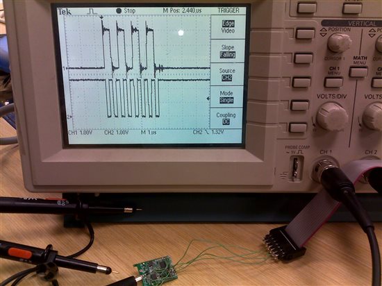
  • Here is the waveform of  SCLK, I don't know why there are only 7 cycles and the last one is much narrower than others, tm=50us while ts=500us.  Moreover, the fsclk is much slower than SMCLK/2, how does this situation happen? When I tested I2C bus, the fsclk is also very slow. It seems that the USCI always makes the cycles much slower than expected SMCLK/2. Could anyone help me to check the waveform is correct or not? Thanks!

  • Lijun,

    The waveform does not look like it is of SMCLK. I would expect SMCLK to look like a (near)perfect square wave. 

    Satbir

  • Hi Satbir,

    Thanks for reply!

    I am very confuse about the waveform, because I select the DCOCLK as the source MCLK and SMCLK, and set the DCO to 8MHz or 16MHz, but the waveforms of  of USCI_B are always the same, i.e. the output of MSP430F2132   Pin3.3.  The code are shown following:

     BCSCTL1 = CALBC1_8MHZ; 
     DCOCTL = CALDCO_8MHZ;
    BCSCTL2 |=0x52;

    OR

    BCSCTL1 =RSEL3 + RSEL2 + RSEL1+ RSEL0;
    DCOCTL =DCO2 + DCO1 + DCO0;
    BCSCTL2 |=0x52;

    Could you capture a waveform of your USCI SCLK, SDI and SDO please if it is convenient  for you.

    Thanks with kind regards!

  • Lijun,

    I did not have the ADXL345 setup, so I just ran the my code without anything connected to the MSP430F2274 and captured wave forms from SDO and SCLK Pins.

    The first waveform is of the data being sent to the SPI. I sent 0xAA(10101010)

    The following waveform is of the SCLK (SPI Clock). SPI was being clocked by SMCLK  at 4 MHz, I verified the frequency of SCLK and it was in fact 4MHz.

    Also in your read the ID part, you need to send a Dummy Byte to receive the Device ID. So it should be:

                                                // Read the ID//
    P3OUT &= ~BIT0;                         // Enable ADXL346, /CS reset

    while ((UCA0STAT & UCBUSY)); // Wait if Busy

    UCB0TXBUF = 0x80;                   // Write address 0x00

    while ((UCA0STAT & UCBUSY)); // Wait if Busy

    UCB0TXBUF = 0xFF                   // Write Dummy byte 0xFF

    while (!(IFG2 & UCB0RXIFG));   // USCI_B0 RX buffer ready?
    data = UCB0RXBUF;                   // data
    P3OUT |= BIT0;                             // Disable ADXL346, /CS set

    Hope this helps.

    Satbir

  • Hi Satbir, 

    Thanks a lot.

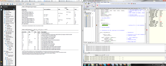
    Considering the 3-wire SPI or 4-wire SPI, your explanation before is a little different from the datasheet of ADXL345, see the snapshot 

    How to distinguish 3-wire or 4-wire? If /CS pin is controlled by any other GPIO,  should the 3-wire SPI diagram above be called '2-wire SPI'? In figure 35,  4 wires are connect to MSP430 here, it is still recognized as 3-wire SPI by MSP430, so we have set 3 PIN SPI in the code. Am I right? Because I have to build a new design to test, so I should better make it clear, and I am sorry to trouble you on this issue.

    How did you power the ADXL345 please? Single-power supply or dual-power supply?  Seperated external power supply or powered by MSP430? And what about the supply voltage, 2.5V or 3.3V please? Forgive me so many questions, I have spent lots time on the communication between MSP430F2132 and ADXL346, but I still cannot read the ID. I don't know what the problem is, so I plan to build a new board which just has MSP430F2132, ADXL345 and ADXL346 to test.

    Thanks for your pictures again, and I'll test my board again on Monday, as I cannot access to our lab at weekend.

    Kind regards,

    Lijun

  • Liljun,

    Don't get confused with the naming conventions. Check the following link:

    http://www.atomicrhubarb.com/filebrowser/download/1451

     3 Wire or 4 Wire are two modes available on  MSP430. On MSP430 3 wire mode uses SDO,SDI and SCLK signals, hence 3 wire, but in reality you will need an other wire for the chip select line (GPIO Pin can be used). So even in 3 pin mode you be using 4 wires. 

    You should be using the mode shown in Figure 35. 

    I powered it with a  separate single 3.3V power supply and i used a breakout board from Sparkfun for the ADXL345. Just make sure that you have the correct clock and data polarity settings on MSP430.

    When you try to read the ID, do you get any data at all?

    Satbir

  • Hi Satbir,

    Thanks for your further explanation!  Now I am clear.

    When I tried to read the ID, I can only get 0x00.

    And today I got the following waveform occasionally, it seems better, but just once. And I tried to redo it again, but I can only get the wave as before. I don't know how it happened and why it disappeared?

    It seems there are much noise, is it introduced by these wires jumped? For this PCB, it is power by the debugger, 2.6V.

    So I plan to rebuild a new prototype and buy a breakout board as well, so I don't need to consider the soldering issue. Thanks!

    Kind regards,

    Lijun

  • Hey Lijun,

    Were you able to fix the problem?

    In this thread i have posted some basic code for ADXL345 with MSP430F2274, that i wrote about 2 years ago.

    http://e2e.ti.com/support/microcontrollers/msp43016-bit_ultra-low_power_mcus/f/166/p/221110/782579.aspx#782579

    See if it could of any help to you.

    Satbir

  • Hi Satbir,

    Thanks a lot! I am testing a new board just with MSP430F2132 on it and an ADXL345 breakout board. With your help I can successfully read the ID 0xE5 each time, it gives me much more encouragement, and thanks you again.

    And also a little confuse about the write function which you wrote 2 years ago, http://e2e.ti.com/support/microcontrollers/msp43016-bit_ultra-low_power_mcus/f/166/p/221110/782579.aspx#782579.  How did you check it was correctly written please? Such as

    // write to the data format//
    spi_on;
    write_byte(0x31,0x07);
    spi_off;
    delay_2;

    // make sure write worked//
    spi_on;
    dataform = read_byte(0xb1);
    spi_off;
    delay_2;

    You wrote data 0x07 to address 0x31, but when you check it you read the address 0xb1. why did you read 0xb1, not 0x31? Where is the address 0xb1? Did I miss some information on the datasheet? 

    Also if it is successfully written in above example, what the correct value of dataform should be please? Is it 0x07 which you just wrote in?

    Sorry about so much questions.

    Kind regards,

    Lijun

  • That's good that you are able to read the device ID correctly!!

    You did miss some information from the data sheet:

     ADXL345 uses a  6 Bit register address(Bit5-Bit0). The Bit7 and Bit6 are there as  command inputs. 

    When the Bit7 is set it tells ADXL345 that the address is being read, and when it is not set it is being written to. 

    So to read from address  0x31, you need to actually send 0xB1. 

    If correctly written then the value read should be equal to value written.

    Hope this clears some doubts.

    Satbir

  • Hi Satbir,

    Thanks a lot! It makes sense.

    Today when I woke up, I suddenly realized why you wrote 0xB1, not  0x31, Just like your explanation above, that's also why write 0x80 to read ID, not 0x00. I don't know what I was thinking yesterday, sorry about that.

    It seems there is some trouble to write, as the value read is not the value written,  It seems only the lower 4 bits is correct. I'll try to find the reason, if i cannot fix it then I seek your help.

    Best Regards,

    Lijunj

  • Hi Satbir,

    Really thank you very much!

    Now I can correctly read and write ADXL345, I cannot get this without your patient and long-time help.

    I could not write correctly days ago, and it was caused by a poor wire connection.

    Thanks again!

    Regards,

    Lijun

  • I am glad that you got it working.

    I was in the same boat when I was doing my project and this Community helped me out. 

    Cheers,

    Satbir

  • Hi!  I am trying to connect the MSP430F5438A wit the ADXL345. I started to build the SPI communication and I want to connect the devices together.

    My goal is to put the Accelerator in some operations by sending commands and then I want to receive

    informations about the position of the axes of x, y and z.  First I started building the communication with all sending commands I want to (also with a interrupt handler, but I had compiling problems.

    Now I reduced the code (commanded all the rest) and I just want to test the communiacation in a simpler way with one sending information and one receiving information.

    Still I cannot compile the code without errors. Can somebody give some advices?

    Thanks.


    #include "msp430x54x.h"                 // einfügen der Mikroprozessordaten
    #include "EHAL\hal_board.h"

    void main (void) // Hauptprogramm starten
    {


      halBoardInit();  
      halBoardStartXT1();    
      halBoardSetSystemClock(SYSCLK_1MHZ);
      halBoardOutputSystemClock();
     
     // init_uart();
     
      while (1)
      {

    WDTCTL=WDTPW+WDTHOLD;    // ausschalten des Watchdogs
    P10SEL=0x0F;        // PSEL, SPI Konfiguration auswählen, 0b00001111
    UCB0CTL1|=UCSWRST;                      // **Put state machine in reset** !!!
    P10DIR=0x0B  ; // SCLK ist 1 auf P10.3 ; MOSI ist 1 auf P10.1 ; SOMI ist 0 auf P10.2, CS(low active) auf 1 am P10.0, 0b00001011
    // P10REN= 0b00000100;// CS quer dauerhaft auf low gesetzt, um die Kommunikation zu bewerkstelligen, keine gute Idee
    UCB3CTL0|=UCSYNC | UCMODE1 | UCMST | UCMSB;     // synchroner Modus, 4 pin SPI einstellen , Master Modus eingestellt, MSB zuerst   
                                      
    UCB3CTL0|=UCSSEL_2;// Zeitgeber auswählen, SMCLK
    // UCB3BR0 = 0x02; // Zeitgeber einstellen, UCA3BR0 und UCA3BR1, (UCAxBR0 + UCAxBR1 × 256)
    // UCB3BR1 = 0;  // später ncoh einmal die Berechnung bedenken und mit den Angaben im Datenblatt vergleichen
    __bis_SR_register(GIE);// globales Interrupt zulassen

    // ?Polarität und Phase der seriellen clock definieren? nur Zusatz

    UCB3CTL1&=~UCSWRST; // Initialisierung der State machine

    UCB3IE|=UCRXIE;// Interrupt zulassen

    spi_senden(0x31,0x4E);
     
    unsigned char spi_empfang(unsigned char receive_byte);


      return;
     
      }


    } // beenden des Hauptprogrammes

    void spi_senden(unsigned char addr,unsigned char data)  //
      {
             P10OUT&=~BIT0;       // CSquer auf low setzen, um die Übertragung anzufangen, nicht P10REN benutzen!
             while(!(IFG3&UCB3TXIFG));   // nicht UCB3IFG benutzen, sondern IFG3
                                             // eventuell das Flag löschen  
                                               
              UCB3TXBUF=addr;                      // Addresse,  0x31;
              delay(10);  // Wartezeit definieren, 10 Zyklen, eventuell zu kurz
          
          while(!(IFG3&UCA3TXIFG));             // nicht UCB3IFG benutzen, sondern IFG3
              UCB3TXBUF=data;  //  SELF_TEST | SPI | INT_INVERT | 0 | FULL_RES | Justify | Range      data sozusagen, Manipulierung, 0b01001110,  0x4E;
              delay(10);  // Wartezeit definieren, 10 Zyklen, eventuell zu kurz
           P10OUT|=BIT0;            // CSquer auf high setzen, um die Übertragung zu beenden}

      };
     
     
        unsigned char spi_empfang(unsigned char receive_byte) // für x Empfangsmetode erstellen, UCA3RXBUF-Inhalt soll empfangenen Daten gefüllt werden
        {                           

                             
        P10OUT&=~BIT0;                         // CSquer auf low setzen, um die Übertragung anzufangen
     
     
          //           Register 0x32-  DATAX0   least significant byte X-axes
       
          while(!(IFG3&UCA3RXIFG));             // nicht UCB3IFG benutzen, sondern IFG3
                                               
                                               
             receive_byte=UCB3RXBUF;                       // Addresse
              delay(10);  // Wartezeit definieren, 10 Zyklen, eventuell zu kurz
     
     
                   IFG3=~UCB3IFG;  // Flag löschen
                   P10OUT|=BIT0;                        // CSquer auf high setzen, um die Übertragung zu beenden}

     
        };

  • Roko Sobar said:
    Still I cannot compile the code without errors. Can somebody give some advices?

    Yes, you could post the exact compiler error messages (and mark their line numbers in the code you posted)

  • Hi!

    The Code is compiled now, but the content of the RXBUF is always 0x00. My goal is to receive the information of the x-, y- and z-axes in

    a stream mode. Is mybe the configuration of the sensor wrong?

    3716.ACC_Measurement.txt
    
    // Basiskommentare f�r die SPI Kommunikation
    
    // #define delay_2 __delay_cycles(10);  // eine andere M�glichkeit ein Delay zu definieren
    
    #include "msp430F5438A.h"                 // einf�gen der Mikroprozessordaten
    #include "stdint.h"
    
    //Variablen
    char addr;
    char data;
    char receive_byte;
    char receive_data;
    
    //Funktionen
    void spi_senden();
    uint8_t spi_empfang();
    uint8_t leseschreib(); //Testmethode f�r den ID-Empfang
    uint8_t koordinatenleseschreib();
    
    
    //Einstellunmgen ADXL345
    void spi_senden_DATA_FORMAT(); 
    void spi_senden_BW_RATE();  
    void spi_senden_FIFO_CTL();
    void spi_senden_POWER_CTL();  // in diesem Register das Measure Bit setzen um eine Messung zu starten
    //void spi_senden_FIFO_STATUS();
    void spi_beenden_POWER_CTL();      // Messung wieder beenden und in den Standby-Modus wieder zur�ckkehren
    
    //Koordinatenachsen x,y,z
    uint8_t DATAX0leseschreib();
    uint8_t DATAX1leseschreib();
    uint8_t DATAY0leseschreib();
    uint8_t DATAY1leseschreib();
    uint8_t DATAZ0leseschreib();
    uint8_t DATAZ1leseschreib();
    
    void main (void) // Hauptprogramm starten
    
    {
    
      WDTCTL=WDTPW+WDTHOLD;    // ausschalten des Watchdogs
      P10SEL|= BIT1 + BIT2 + BIT3;                         //P10SEL|=0x0F;        // PSEL, SPI Konfiguration ausw�hlen, 0b00001111
      UCB3CTL1|=UCSWRST;                      // **Put state machine in reset** !!!
      P10DIR|= BIT0;             //P10DIR|=0x0D; // SCLK ist 1 auf P10.3 ; MOSI ist 1 auf P10.1 ; SOMI ist 0 auf P10.2, CS(low active) auf 1 am P10.0, 0b00001101
    
    // P10REN= 0b00000100;// CS quer dauerhaft auf low gesetzt, um die Kommunikation zu bewerkstelligen, keine gute Idee
    
      UCB3CTL0|=UCSYNC | UCMST | UCMSB | UCCKPL; //| UCMODE0;   // synchroner Modus, 4 pin SPI einstellen , Master Modus eingestellt, MSB zuerst   
      UCB3CTL1|=UCSSEL_2;  // Zeitgeber ausw�hlen, SMCLK 
      UCB3BR0=0x02;       //Zeitgeber einstellen, UCA3BR0 und UCA3BR1, (UCAxBR0 + UCAxBR1 ? 256)
      UCB3BR1=0;  // spaeter ncoh einmal die Berechnung bedenken und mit den Angaben im Datenblatt vergleichen
    
      UCB3CTL1&=~UCSWRST; // Initialisierung der State machine
      UCB3IE|=UCRXIE + UCTXIE;// Interrupt zulassen


      while (1)
      {
      //leseschreib();                         // als Test soll die ID gesendet werden


     //Einstellungen ADXL345 im Standby-Modus
    // spi_beenden_POWER_CTL();  // Measure Bit auf 0 setzen  
        
    // leseschreib();    
    spi_senden_DATA_FORMAT(); 
    spi_senden_BW_RATE();  
    spi_senden_FIFO_CTL(); 
    spi_senden_POWER_CTL(); // hier die Messung starten 
    
    //spi_senden_FIFO_STATUS();  
      
     // Koordinatenachsen x,y,z
    DATAX0leseschreib();  // LSb X-Achse
    DATAX1leseschreib();  // MSb X-Achse
    DATAY0leseschreib();  // LSb X-Achse
    DATAY1leseschreib();  // MSb X-Achse
    DATAZ0leseschreib();  // LSb Z-Achse
    DATAZ1leseschreib();  // MSb Z-Achse


    spi_beenden_POWER_CTL(); // hier die Messung wieder beenden und in den Standby-Modus setzen   
                             // Measure Bit auf 0 setzen
    
    //      spi_senden();                                
    
      }
    
      
    } // beenden des Hauptprogrammes
    
    
    // Register 0x31- DATA_FORMAT  (DATA format control)
    
    void spi_senden_DATA_FORMAT()  
    {
           // P10OUT&=~BIT0;                          // CSquer auf low setzen, um die �bertragung anzufangen, bei 4 wire


            while(!(UCB3IFG&UCTXIFG));       // nicht UCB3IFG benutzen, sondern IFG3, wieder zur�ck ge�ndert
                                            // eventuell das Flag l�schen  
            UCB3TXBUF=0x31;                      // Addresse,  0x31; 
            __delay_cycles(10);  // Wartezeit definieren, 10 Zyklen, eventuell zu kurz
          
            while(!(UCB3IFG&UCTXIFG));             // nicht UCB3IFG benutzen, sondern IFG3
    
            UCB3TXBUF=0x4E;  //  SELF_TEST | SPI | INT_INVERT | 0 | FULL_RES | Justify | Range      data sozusagen, Manipulierung, 0b01001110,  0x4E; 
    
            __delay_cycles(10);  // Wartezeit definieren, 10 Zyklen, eventuell zu kurz
    
    };       
      //---------------------------------------------------------------------------------------------------          
           
       // Register 0x2C BW_RATE  (Data rate and power mode control) 
    
     void spi_senden_BW_RATE()  
    
     {    while (!(UCB3IFG&UCTXIFG));           // UCB3IFG benutzen
    
                                       
             UCB3TXBUF=0x2C;                       // Addresse
    
             __delay_cycles(10);  // Wartezeit definieren, 10 Zyklen, eventuell zu kurz   
    
          while (!(UCB3IFG&UCTXIFG));           // UCB3IFG benutzen, sondern IFG3
    
             UCB3TXBUF = 0x0A;                    //  0 | 0 | 0 | LOW_POWER | Rate | Rate   , Rate auf 100 Hz,data, Manipulierung, 0b00001010
    
             __delay_cycles(10);  // Wartezeit definieren, 10 Zyklen
     };       
       //----------------------------------------------------------------------------------------------------------    
           
        // Register 0x38- FIFO_CTL 
    
    void spi_senden_FIFO_CTL()   
    
    {     while (!(UCB3IFG & UCTXIFG));               // UCB3IFG benutzen
    
                                               
              UCB3TXBUF = 0x38;                       // Addresse
    
             // __delay_cycles(10);  // Wartezeit definieren


         while (!(UCB3IFG & UCTXIFG));              // nicht UCB3IFG benutzen, sondern IFG3
    
              UCB3TXBUF = 0x80 ;    //  FIFO_MODE | FIFO_MODE | Trigger | Samples | Samples  | Samples | Samples | Samples    data sozusagen, Manipulierung, 0b10000000
    
              __delay_cycles(10);  // Wartezeit definieren, 10 Zyklen  
    };
    
    
              // Register 0x2D- POWER_CTL   
    
    void spi_senden_POWER_CTL() 
    
    {     while (!(UCB3IFG&UCTXIFG));               // UCB3IFG benutzen
                                             
              UCB3TXBUF=0x2D;                       // Addresse
    
              __delay_cycles(10);  // Wartezeit definieren, 10 Zyklen, eventuell zu kurz
    
          while (!(UCB3IFG&UCTXIFG));
    
              UCB3TXBUF=0x04 ;    //  0 | 0 | Link | AUTO_SLEEP | Measure | Sleep | Wakeup          data sozusagen, Manipulierung, 0b0000100
    
              __delay_cycles(10);  // Wartezeit definieren, 10 Zyklen
    };
    
    // Messung beenden und wieder in den Standby-Modus zur�ckkehren
    
    void spi_beenden_POWER_CTL() 
    
    {     while (!(UCB3IFG&UCTXIFG));               // UCB3IFG benutzen
                                             
              UCB3TXBUF=0x2D;                       // Addresse
    
              __delay_cycles(10);  // Wartezeit definieren, 10 Zyklen, eventuell zu kurz
    
          while (!(UCB3IFG&UCTXIFG));
    
              UCB3TXBUF=0x00;    //  0 | 0 | Link | AUTO_SLEEP | Measure | Sleep | Wakeup          data sozusagen, Manipulierung, 0b0000100
    
              __delay_cycles(10);  // Wartezeit definieren, 10 Zyklen
    };


                    // Register 0x39-  FIFO_STATUS  
    //void spi_senden_FIFO_STATUS() 
    //   
    //
    //{     while (!(UCB3IFG&UCTXIFG));                // nicht UCB3IFG benutzen
    //                                         
    //
    //          UCB3TXBUF=0x39;                       // Addresse
    //
    //          __delay_cycles(10);  // Wartezeit definieren, 10 Zyklen, eventuell zu kurz
    //
    //      while (!(UCB3IFG&UCTXIFG));   // UCB3IFG benutzen
    //
    //         UCB3TXBUF=;    //   
    //
    //       __delay_cycles(10);  // Wartezeit definieren, 10 Zyklen
    //};  
    //  //--------------------------------------------------------------------------------------------------------- 
    
    
    //-------------------------------------------------------------------------------
    
    // Testmethode zum einlesen der ID
    
    //uint8_t leseschreib()
    //
    //{                                                // Beginn der Funktion
    //  
    //  P10OUT &= ~BIT0;
    //  
    //  while (!(UCB3IFG&UCTXIFG));
    //
    //  UCB3TXBUF = 0x00; // 0x41 // Test mit 0x80;
    //
    //
    // __delay_cycles(10);
    // 
    // 
    // while(!(UCB3IFG&UCRXIFG)); 
    // 
    // 
    // return(UCB3RXBUF);
    //
    //}; 
    
    //-------------------------------------------------------------------------------
      
    // Methode zum einlesen der Koordinatenwerte  DATAX0
    
    uint8_t DATAX0leseschreib()                              // Register 0x32-    DATAX0  least significant byte X-axes
    {                                                
      
      P10OUT &= ~BIT0;
      
       while (!(UCB3IFG&UCTXIFG));
    
          UCB3TXBUF = 0x32; // Register 0x32-  DATAX0   least significant byte X-axes
    
    
          __delay_cycles(10);
     
     
      while(!(UCB3IFG&UCRXIFG)); 
     
     
          __delay_cycles(10); 
     
     UCB3IFG&=~UCRXIFG;
          
     return(UCB3RXBUF);
    
    }; 
    
    //-------------------------------------------------------------------------------
    
    // Methode zum einlesen der Koordinatenwerte  DATAX1       
             
    uint8_t DATAX1leseschreib()             // Register 0x33-    DATAX1    most significant byte X-axes
    
    {              
          while (!(UCB3IFG&UCTXIFG));           // UCB3IFG benutzen
                                            
    
               UCB3TXBUF=0x33;                       // Addresse
    
            __delay_cycles(10);  // Wartezeit definieren, 10 Zyklen, eventuell zu kurz
     
    
          while (!(UCB3IFG&UCRXIFG));                  // nicht UCB3IFG benutzen 
    
              __delay_cycles(10);  
      
      return(UCB3RXBUF);
              
    };
    
     //---------------------------------------------------------------------------------------------------------                 
    
                
     // Methode zum einlesen der Koordinatenwerte  DATAY0 
    
    uint8_t DATAY0leseschreib()        // Register 0x34-  DATAY0  least significant byte  Y-axes
    
    {
         while (!(UCB3IFG&UCTXIFG));                
         
              UCB3TXBUF=0x34;                       // Addresse
    
              __delay_cycles(10);  // Wartezeit definieren, 10 Zyklen, eventuell zu kurz
    
         
        while (!(UCB3IFG&UCRXIFG));               // nicht UCB3IFG benutzen, sondern IFG3
    
           __delay_cycles(10);  // Wartezeit definieren, 10 Zyklen
            
      return(UCB3RXBUF);
      
    }; 
    
      //---------------------------------------------------------------------------------------------------------         
    
    // Methode zum einlesen der Koordinatenwerte  DATAY1 
    
    uint8_t DATAY1leseschreib()  // Register 0x35-  DATAY1  moct significant byte  Y-axes
      
    {
         while (!(UCB3IFG&UCTXIFG));               // nicht UCB3IFG benutzen
                                            
            UCB3TXBUF=0x35;                       // Addresse
    
            __delay_cycles(10);  
         
    
        while (!(UCB3IFG&UCTXIFG));              // nicht UCB3IFG benutzen   
    
            __delay_cycles(10);  
    
        return(UCB3RXBUF);
             
    };
    
     // ---------------------------------------------------------------------------------------------------------        
    
    // Methode zum einlesen der Koordinatenwerte  DATAZ0 
    
      
    //    Register 0x36-  DATAZ0  least significant byte  Z-axes
    
    uint8_t DATAZ0leseschreib()
    
    {
       while (!(UCB3IFG&UCTXIFG));            // UCB3IFG benutzen
                                            
    
             UCB3TXBUF=0x36;                       // Addresse
    
             __delay_cycles(10);  // Wartezeit definieren
       
    
     while (!(UCB3IFG&UCTXIFG));            // nicht UCB3IFG benutzen  
    
             __delay_cycles(10);  // Wartezeit definieren
             
     return(UCB3RXBUF);
    };
    
      //---------------------------------------------------------------------------------------------------------     
    
    // Methode zum einlesen der Koordinatenwerte  DATAZ1 
    
    
                    // Register 0x37-  DATAZ1  most significant byte  Z-axes
    uint8_t DATAZ1leseschreib()
    {
          while (!(UCB3IFG&UCTXIFG));              // UCB3IFG benutzen
                                           
               UCB3TXBUF=0x37;                   
    
              __delay_cycles(10);  
    
          while (!(UCB3IFG&UCTXIFG));                  // UCB3IFG benutzen
    
             __delay_cycles(10);  // Wartezeit definieren
    
    return(UCB3RXBUF);
    
     };
             
     //--------------------------------------------------------------------------------------------------------- 


    //         IFG3=~UCB3IFG;  // Flag l�schen
    
    //         P10OUT |= BIT0;                        // CSquer auf high setzen, um die �bertragung zu beenden}
    
    
    //// 3 verschiedene Felder f�r die �bertragung definieren, Informationen f�r die x-,y-,z-Achsen


    //} // Beenden der Methode


    Thanks and greetings.

  • I see many delays that aren't necessary. You check for TXIFG which is sufficient.
    You only need delays at two points: after asserting CS (see the ADXL datasheet for minimum delay between CS_>0 and first clock pulse) and before de-asserting CS (again, see datasheet). And, before the delay at de-asserting CS, ensure that UCBUSY is clear, that means, everyhtign you stuffe dinto TXBUF has been sent.

    Anothe rproblem: each time you sent a byte to the ADXL, you also received a byte. So when you really want to receive something, you already have in RXBUF what you received while sending the last command. Also, after sending a command, what you received is received whiel the slave hasn't seen your command. it is NOT the answer. The answer comes with the next (dummy) byte you send.

    uint8_t DATAX0leseschreib()
    {                                               
      P10OUT &= ~BIT0;             // after setting CS to 0, you should insert a delay, depending on the slave specs.
       while (!(UCB3IFG&UCTXIFG)); // this only means RXBUF is empty. But whatever you may have sent before might still be sending
                                   // you should wait for UCBUSY=0

          UCB3TXBUF = 0x32;        // send 0x32
          __delay_cycles(10);      // superfluous
      while(!(UCB3IFG&UCRXIFG));   // here you're waiting for what has been received while the byte before the 0x32 was sent.
                                   // After you waited for UCBUSY=0 above, you need to clear RXIFG, then wait for thee byte received during
                                   // sending 0x32, clear RXIFG, then send a dummy byte in order to reeive your result.

          __delay_cycles(10);      // superfluous
     UCB3IFG&=~UCRXIFG;            // superfluous, reading UCB3RXBUF in teh resturn statement will already clear the RXIFG bit
     return(UCB3RXBUF);            // what about CS? Shouldn't it be set to 1 after communication?
    };

  • Thanks for the critic and the helping comments.

      I reduced the code and I tried to improve it, but it is still not working correctly. No correct data in the Receive buffer.

    Maybe Jens you can give me some support.

    I tried to figure out the correct number for the delay cycles, but I must admit I do not know how to figure out the right constant for the function.

    t delay is about 5 ns and tquiet also about 5 ns. Shold the function be then __delay_cycles(5); ?

    Thanks and Greetings!

  • 5621.ACC_Code3 .txt
    
    //  SPI Communication
    
    
    #include "msp430F5438A.h"                 // einf�gen der Mikroprozessordaten
    #include "stdint.h"
    
    //Variables
    uint8_t addr;
    uint8_t data;
    uint8_t Test;
    uint8_t receive_byte;
    uint8_t receive_data;
    
    //Settings of the ADXL345
    
    uint8_t testreadwrite(); 
    
    //void spi_senden_CONFG();
    
    //Coordinate axes x,y,z
    //uint8_t DATAX0readwrite();                                    // DATAX0  
    
    
    void main (void)                                              // Starting main program
    
    {
    
      WDTCTL=WDTPW+WDTHOLD;                                       // turn of the Watchdogs
      
      P10SEL|= BIT0 + BIT1 + BIT2 + BIT3;                               //P10SEL|=0x0F;    // SCLK, BIT3, P10.3 ; MOSI ist 1 auf P10.1 ; SOMI ist 0 auf P10.2, CS(low active) auf 1 am P10.0, 0b00001101  // PSEL, SPI Konfiguration ausw�hlen, 0b00001111
      P10DIR|=0x40;                                              //P10DIR|=0x0D;  //GPIO-Pin 10.6, defining the direction, output
      
      UCB3CTL1|=UCSWRST;                                          // **Put state machine in reset** !!!
      UCB3CTL0|= UCSYNC | UCMST | UCMSB | UCCKPL | UCMODE1;       // synchronous Mode,3 pin SPI,  (4 pin SPI, old), Master Mode, MSB first   
      UCB3CTL1|=UCSSEL_2;                                         // SMCLK 
      UCB3BR0|=0x02;                                              // Rate, UCA3BR0 and UCA3BR1, (UCAxBR0 + UCAxBR1 ? 256)
      UCB3BR1=0;                                               
      UCB3IE|=UCRXIE + UCTXIE;                                    // Interrupts enable
      UCB3CTL1&=~UCSWRST;                                         // Initialising of the State machine
    
     // spi_senden_CONFG();  
      
      while (1)
      {                       


        //spi_senden_CONFG();
        
       testreadwrite();
       //DATAX0readwrite();                                    // DATAX0  
         __delay_cycles(5);   
         P10OUT|=BIT6;                                            // putting CS to 1 to end transmission
      } 
    } // end main program
    
    
    //// Testfunction for SPI, receiving ID of the ADXL345
    
    uint8_t testreadwrite()                                    // Testfunction   
    {                                                
           P10OUT &= ~BIT6;					   // CS putting to low to start transmission
            __delay_cycles(5);                                 // inserting a delay
       
        while (!(UCA0STAT & UCBUSY)==0);                       //    while (UCBUSY!=0));
              UCB3TXBUF = 0x80;                                // sending 
              UCB3IFG &=~UCTXIFG;                              // clearing the flag
        while (!(UCA0STAT & UCBUSY)==0);  
              UCB3TXBUF=0xFF;                                 // sending dummy byte
              UCB3IFG &=~UCTXIFG;   
                                           
     return(UCB3RXBUF);
                                                              // putting CS to 1 in the while loop outside of the function
    }; 


    //Configuration
    
    //void spi_senden_CONFG()
    //{
    //        P10OUT &= ~BIT6;	                // CSquer to low setzen, starting configuration
    //    
    //        while (!(UCA0STAT & UCBUSY)==0);      // waiting
    //                                             
    //        UCB3TXBUF=0x31;                       // Addresse,  0x31; 
    //        UCB3IFG &=~UCTXIFG;
    //        while (!(UCA0STAT & UCBUSY)==0);      // waiting
    //        UCB3TXBUF=0x4E;                       //SELF_TEST | SPI | INT_INVERT | 0 | FULL_RES | Justify | Range      data sozusagen, Manipulierung, 0b01001110,  0x4E; 
    //        UCB3IFG &=~UCTXIFG;   
    
    //        
    //        while (!(UCA0STAT & UCBUSY)==0);      // waiting
    //        UCB3TXBUF=0x2C;                       // Addresse
    //        UCB3IFG &=~UCTXIFG;
    //        while (!(UCA0STAT & UCBUSY)==0);     // finished?
    //        UCB3TXBUF = 0x0A;       
    //        UCB3IFG &=~UCTXIFG;
    
    //
    //        while (!(UCA0STAT & UCBUSY)==0);     // waiting
    //        UCB3TXBUF = 0x38;                    // Addresse
    //        UCB3IFG &=~UCTXIFG;
    //        while (!(UCA0STAT & UCBUSY)==0);     // waiting
    //        UCB3TXBUF = 0x80 ;                   //  FIFO_MODE | FIFO_MODE | Trigger | Samples | Samples  | Samples | Samples | Samples    data sozusagen, Manipulierung, 0b10000000
    //        UCB3IFG &=~UCTXIFG;
     
    //        
    //        while (!(UCA0STAT & UCBUSY)==0);     // waiting
    //        UCB3TXBUF=0x2D;                      // Addresse
    //        UCB3IFG &=~UCTXIFG;
    //        while (!(UCA0STAT & UCBUSY)==0);     // waiting
    //        UCB3TXBUF=0x04 ;                     //  0 | 0 | Link | AUTO_SLEEP | Measure | Sleep | Wakeup          data sozusagen, Manipulierung, 0b0000100
    //        UCB3IFG &=~UCTXIFG;
    //        
    //        
    //        __delay_cycles(5); 
    //        
    //        P10OUT|=BIT6;                        //         
    //};
    
    //uint8_t DATAX0readwrite()                                    // DATAX0   
    //{                                                
    //       P10OUT &= ~BIT6;					   // CS putting to low to start transmission
    //        __delay_cycles(5);                                 // inserting a delay
    //   
    //    while (!(UCA0STAT & UCBUSY)==0);                       //    while (UCBUSY!=0));
    //          UCB3TXBUF = 0x32;                                // sending 
    //          UCB3IFG &=~UCTXIFG;                              // clearing the flag
    //    while (!(UCA0STAT & UCBUSY)==0);  
    //          UCB3TXBUF=0xFF;                                 // sending dummy byte
    //          data= UCB3RXBUF 
    //          UCB3IFG &=~UCTXIFG;   
    //                                       
    // return(data);
    //                                                          // putting CS to 1 in the while loop outside of the function
    //}; 


    I forgot to add the code to my comment. I tried to read the ID and I set a Breakpoint. Most of the times I ran the program it worked ok, but sometimes not.

    Could the Delay be a problem? I Tried it with __delay_cycles(5).  I have putted a configuration method in the code. Is the method ok like this?

    Later (if the testread-function is ok I want to replace it by reading the value of the coordinates( at the bottom of the code there is a commented example for X0).

    Could it work out like this? Advices?

    Greetings

  • Roko Sobar said:
    t delay is about 5 ns and tquiet also about 5 ns. Shold the function be then __delay_cycles(5); ?

    5ns is the cycle time of a 200MHz CPU. It is impossible to not have at least 120ns between CS going low and the first clock edge, even if you write 0x00 to TXBUF, using the constant generator (which still would take three MCLK cycles, which are 3*40ns @25MHz). So that isn't a problem.
    However, you must be sure that the USCI is done sending before you rise CS again. You don't need a fixed-time delay here too, you only have to check for UCBUSY bit.

    Some things about your code:

      UCB3IE|=UCRXIE + UCTXIE;                                    // Interrupts enable
      UCB3CTL1&=~UCSWRST;                                         // Initialising of the State machine

    while UCSWRST is set, you can't set the IE bits. I guess this is intentionally, since SWRST sets UCTXIFG, and with UCTXIE set too but the stat emachine in reset, this would lead to an eternal itnerrupt loop.
    But luckily your setting of these bits has noeffect, because you don#t have any ISR edfined to handle the interrupts. THis would crash your MSP if the bits were set.

              UCB3TXBUF = 0x80;                                // sending
              UCB3IFG &=~UCTXIFG;                              // clearing the flag
    Clearing the flag is superfluous, as writing to TXBUF automatically clears it.

              UCB3TXBUF=0xFF;                                 // sending dummy byte
              UCB3IFG &=~UCTXIFG;   
           return(UCB3RXBUF);

    After writing to TXBUF, you'll have to wait until the dummy 0xff is sent before you can read the answer from RXBUF. You return what was received somewhen sooner.
    Put another while loop before you return.
    Also, you may replace the second while loop from waiting for UCBUSY to waiting for RXIFG. This speeds up the transfer a little bit.

  • Hi Jens!

    0572.7.5.2013 ACC_.txt
    ///  SPI Communication
    
    
    #include "msp430F5438A.h"                                     // microprozessor 
    #include "stdint.h"
    
    //Variables
    uint8_t addr;
    uint8_t dataX0;
    uint8_t dataX1;
    uint8_t dataY0;
    uint8_t dataY1;
    uint8_t dataZ0;
    uint8_t dataZ1;
    uint8_t Test;
    uint8_t receive_byte;
    uint8_t receive_data;
    
    //Settings of the ADXL345
    
    uint8_t testreadwrite(); 
    
    void spi_senden_CONFG();
    
    void main (void)                                                // Starting main program
       
    {
    
       WDTCTL=WDTPW+WDTHOLD;                                        // turn of the Watchdogs
      
      P10SEL|= BIT0 + BIT1 + BIT2 + BIT3;                               //P10SEL|=0x0F;    // SCLK, BIT3, P10.3 ; MOSI ist 1 auf P10.1 ; SOMI ist 0 auf P10.2, CS(low active) auf 1 am P10.0, 0b00001101  // PSEL, SPI Konfiguration ausw�hlen, 0b00001111
      P10DIR|=0x40;                                                 //P10DIR|=0x0D;  //GPIO-Pin 10.6, defining the direction, output
      
      UCB3CTL1|=UCSWRST;                                            // **Put state machine in reset** !!!
      UCB3CTL0|=UCSYNC | UCMST | UCMSB | UCCKPL | UCCKPH | UCMODE1;       // synchronous Mode,3 pin SPI,  (4 pin SPI, old), Master Mode, MSB first   
      UCB3CTL1|=UCSSEL_2;                                           // SMCLK 
      UCB3BR0|=0x02;                                                // Rate, UCA3BR0 and UCA3BR1, (UCAxBR0 + UCAxBR1 ? 256)
      UCB3BR1=0;                                               
     
      UCB3CTL1&=~UCSWRST;                                           // Initialising of the State machine


      while (1)
      
     {                       


      testreadwrite();
    
      }


    uint8_t testreadwrite()                                        // Testfunction   
    {                                                
            P10OUT&=~BIT6;					       // CS putting to low to start transmission
            __delay_cycles(1);                                     // inserting a delay
       
        while (!(UCB3STAT&UCBUSY)==0);                             //    while (UCBUSY!==0));
               UCB3TXBUF=0x80;                                     // sending  


        while (!(UCB3STAT&UCBUSY)==0); 
               //    while( (UCB3IFG&UCRXIFG) == 0);
               //  receive_data=UCB3RXBUF;  //eingebaut
                UCB3TXBUF=0xFF;                                   // sending dummy byte
               //while (!(UCB3IFG&UCRXIFG));  
        while (!(UCRXIFG)); 
                
                receive_data=UCB3RXBUF;  //erg�nzt
                __delay_cycles(1);   
                P10OUT|=BIT6;                              
     return(receive_data);
                                                                 // putting CS to 1 in the while loop outside of the function
    }; 
    

    Thanks for the comments and help! I changed parts of the code and now I am receiving 0xC7 instead of the right ID. Also in the first run I can just see 0x00 in the variable.

    I removed the interrupt stuff. Thanks.

    What is the differenz between UCB3CTL1|=UCSSEL_2;and UCB3CTL1|=UCSSEL_3;  ? Both refer to the SMCLK.

    Greetings!

  • Hi Jens!

    Can you take a look on this Code.

    8508.7.5.2013 17.19 Uhr.txt
    ///  SPI Communication
    
    
    #include "msp430F5438A.h"                 // einf�gen der Mikroprozessordaten
    #include "stdint.h"
    
    //Variables
    uint8_t addr;
    uint8_t dataX0;
    uint8_t dataX1;
    uint8_t dataY0;
    uint8_t dataY1;
    uint8_t dataZ0;
    uint8_t dataZ1;
    uint8_t Test;
    uint8_t receive_byte;
    uint8_t receive_data;
    uint8_t data;
    //uint8_t config = 0xFF & ~BIT6;
    
    //Settings of the ADXL345
    
    uint8_t testreadwrite(); 
    
    void spi_senden_CONFG();
    
    //Coordinate axes x,y,z
    //uint8_t DATAX0readwrite();                                               // DATAX0  
    //uint8_t DATAX1readwrite();                                               // DATAX1 
    //uint8_t DATAY0readwrite();                                               // DATAY0 
    //uint8_t DATAY1readwrite();                                               // DATAY1 
    //uint8_t DATAZ0readwrite();                                               // DATAZ0 
    //uint8_t DATAZ1readwrite();                                               // DATAZ1 
    
    void main (void)                                                           // Starting main program
    
    {
    
       WDTCTL=WDTPW+WDTHOLD;                                                   // turn of the Watchdogs
      
      P10SEL|= BIT0 + BIT1 + BIT2 + BIT3;                                      //P10SEL|=0x0F;    // SCLK, BIT3, P10.3 ; MOSI ist 1 auf P10.1 ; SOMI ist 0 auf P10.2  // PSEL, SPI Konfiguration ausw�hlen, 0b00001111
      P10DIR|=0x40;                                                            //P10DIR|=0x0D;  //GPIO-Pin 10.6, defining the direction, output
      
      UCB3CTL1|=UCSWRST;                                                       // **Put state machine in reset** !!!
      UCB3CTL0|=UCSYNC | UCMST | UCMSB | UCCKPL | UCCKPH | UCMODE1;            // synchronous Mode,3 pin SPI,  (4 pin SPI, old), Master Mode, MSB first   
      UCB3CTL1|=UCSSEL_2;                                                      // SMCLK 
      UCB3BR0|=0x02;      //0x02;     //    10;                                // Rate, UCA3BR0 and UCA3BR1, (UCAxBR0 + UCAxBR1 ? 256)
      UCB3BR1=0;                                               
     
      UCB3CTL1&=~UCSWRST;                                                      // Initialising of the State machine
    
     // spi_senden_CONFG();  
      
      while (1)
      {                       


     //   spi_senden_CONFG();
      
      testreadwrite();
     //  DATAX0readwrite();                                    // DATAX0  
       //DATAX1readwrite();                                    // DATAX1
       //DATAY0readwrite();                                    // DATAY0
       //DATAY1readwrite();                                    // DATAY1
       //DATAZ0readwrite();                                    // DATAZ0
       //DATAZ1readwrite();                                    // DATAZ1
       
     
    // //Testarea
    // // in Standby Mode
    //        UCB3TXBUF=0x31;                       // Addresse,  0x31; DATA_FORMAT, wake up from standby
    //        UCB3IFG &=~UCTXIFG;
    //        while (!(UCB3STAT & UCBUSY)==0);      // waiting
    //        UCB3TXBUF=0x4E;                       //SELF_TEST | SPI | INT_INVERT | 0 | FULL_RES | Justify | Range      data sozusagen, Manipulierung, 0b01001110,  0x4E; 
    //        UCB3IFG &=~UCTXIFG;   
    // 
    // // Ending Meassurement
    // 
    //        while (!(UCB3STAT & UCBUSY)==0);     // waiting
    //        UCB3TXBUF=0x2D;                      // Addresse  POWER_CTRL, switch to measurement
    //        UCB3IFG &=~UCTXIFG;
    //        while (!(UCB3STAT & UCBUSY)==0);     // waiting
    //        UCB3TXBUF=0x04 ;                     //  0 | 0 | Link | AUTO_SLEEP | Measure | Sleep | Wakeup          data sozusagen, Manipulierung, 0b0000100
    //        UCB3IFG &=~UCTXIFG;
    // 
    // 
    // 
    // 
    // 
    // 
    // 
    // 
    // 
    //   
    //     __delay_cycles(10);   
    //     P10OUT|=BIT6; 
    //                                                        // putting CS to 1 to end transmission
    //   
    // 
    //   
     } 
    } // end main program
    
    
    //------------------------------------------------------------------------------------------------------------------------
    
    uint8_t testreadwrite()                                  // Testfunction   
    {                                                
        P10OUT&=~BIT6;			                 // CS putting to low to start transmission
                                                             //     __delay_cycles(10);       // inserting a delay
        
        while (!(UCB3STAT&UCBUSY)==0);                       // while (UCBUSY!==0));
               UCB3TXBUF=0x31;                               // DATA Format Register adress
       
        while (!(UCB3STAT&UCBUSY)==0);      
              UCB3TXBUF=0x00;                                // setting every BIT to 0, BIT=0 means 4 wire communication, sending


        while (!(UCB3STAT&UCBUSY)==0);                       // while (UCBUSY!==0));
               UCB3TXBUF=0x80;                               // sending 


        while (!(UCB3STAT&UCBUSY)==0); 
                                                             // while( (UCB3IFG&UCRXIFG) == 0);
                                                             // receive_data=UCB3RXBUF;  //eingebaut
                UCB3TXBUF=0xFF;                              // sending dummy byte
                                                             //while (!(UCB3IFG&UCRXIFG));  
        while (!(UCTXIFG)); 
                
                receive_data=UCB3RXBUF;  //erg�nzt
                                                             //    __delay_cycles(2);   
         P10OUT|=BIT6;                                       // P10OUT&=~BIT6;                            
     return(receive_data);
                                                             //  return (UCB3RXBUF);  // putting CS to 1 in the while loop outside of the function
    }; 

    Thanks and Greetings

  • Roko Sobar said:
    now I am receiving 0xC7 instead of the right ID

    what do you expect as 'right ID'?

    In your latest code, are you sure about UCCKPH and UCCKPL? There are four possible combinations of the two. Picking the wrong one will cause partially failure, shifted bits (in both write and read) or no success at all.

    UCCKPL but not UCCKPH is a common combination. Note that the meaning of UCCKPL is inverse to the often used motorola SPI notation.

    Roko Sobar said:
    from your code:
    uint8_t testreadwrite()                                  // Testfunction   
    {                                                
        P10OUT&=~BIT6;                                       // CS putting to low to start transmission
                                                             //     __delay_cycles(10);       // inserting a delay
        while (!(UCB3STAT&UCBUSY)==0);                       // while (UCBUSY!==0));
               UCB3TXBUF=0x31;                               // DATA Format Register adress
        while (!(UCB3STAT&UCBUSY)==0);      
              UCB3TXBUF=0x00;                                // setting every BIT to 0, BIT=0 means 4 wire communication, sending
        while (!(UCB3STAT&UCBUSY)==0);                       // while (UCBUSY!==0));
               UCB3TXBUF=0x80;                               // sending
        while (!(UCB3STAT&UCBUSY)==0);
                                                             // while( (UCB3IFG&UCRXIFG) == 0);
                                                             // receive_data=UCB3RXBUF;  //eingebaut
                UCB3TXBUF=0xFF;                              // sending dummy byte
                                                             //while (!(UCB3IFG&UCRXIFG));  
        while (!(UCTXIFG));
                receive_data=UCB3RXBUF;  //ergänzt
         P10OUT|=BIT6;                                      // P10OUT&=~BIT6;                            
     return(receive_data);                                  //  return (UCB3RXBUF);  // putting CS to 1 in the while loop outside of the function
    };

    This code flow is still not correct. The last whiel still doesn't wait until the answer is received. Also, the first lines are not logical. You lower CS but then you wait for SPI going idle. If it weren't already, CS would be low already and you wouldn't need to check for busy, or it might be busy, then you'll have to do more than waiting.
    Also, "while(!UCTXIFG)" is always false, since UCTXIFG is a constant and != 0.
    Try this:

    uint8_t testreadwrite()                                  // Testfunction   
    {                                                
        if(UCB3STAT&UCBUSY){               // for some reason, the SPI is still busy. Normally, it shouldn't, so this whole IF block might be superfluous
            while(UCB3STAT&UCBUSY);        // wait until SPI is idle
            P10OUT |= BIT6;                // de-assert CS, ending ht eprevious transfer
            __delay_cycles(10);            // give the slave some time (see datasheet how much is required between raising and next falling CS)
        }
        P10OUT&=~BIT6;                                // CS putting to low to start transmission

        UCB3TXBUF=0x31;                               // DATA Format Register adress (if the USCI was idle, it now still is, and TXBUF can be written to)
        while (!(UCB3IFG&UCTXIFG));                   // is TXBUF empty (previous byte is sending) yet? On high SPI clock, it would, as teh USCI was idle and should start sending the previous byte immediately, leavign TXBUF empty. But be safe...
        UCB3TXBUF=0x00;                               // setting every BIT to 0, BIT=0 means 4 wire communication, sending
        while (!(UCB3IFG&UCTXIFG));                   // is TXBUF empty (previous byte is sending) yet?
        UCB3TXBUF=0x80;                               // sending

        while (!(UCB3IFG&UCTXIFG));                   // is TXBUF empty (previous byte is sending) yet?
        UCB3TXBUF=0xFF;                               // sending dummy byte
        while (!(UCB3STAT&UCBUSY)==0);                // wait until all sending and receiving is complete
        P10OUT|=BIT6;                                 // de-assert CS
     return(UCB3RXBUF);                               // return (UCB3RXBUF);
    };

  • Hi Jens!

    Thanks for the critic and help again. I will follow your proposals and try to improve the code.

    In fact it is not necessary to config the DATA_FORMAT Register for SPI 4 wire. It is per default in 4 wire.

    In the meantime a new code was developed which was able to receive constantly the right ID of 0xE5.

    3872.8.5.2013_ACC_CODE_Interrupts_ID.txt
    #include "msp430x54xA.h"
    #include "hal_MSP-EXP430F5438.h"
    #include "hal_lcd.h"
    #include <stdint.h>
    #include "hal_pmm.h"
    
    #define SYSTEM_CLOCK    23986176
    
    #define USB_PORT_OUT      P5OUT
    #define USB_PORT_SEL      P5SEL
    #define USB_PORT_DIR      P5DIR
    #define USB_PORT_REN      P5REN
    #define USB_PIN_TXD       BIT6
    #define USB_PIN_RXD       BIT7
    #define USB_PORT_BAUDRATE            57600
    
    #define UART_A3_PSEL                P10SEL
    #define UART_A3_PDIR                P10DIR
    #define UART_A3_TXD_MASK            BIT4
    #define UART_A3_RXD_MASK            BIT5
    
    #define UART_A3_BAUDRATE            57600
    
    char rxBuffer[256];     //Buffer to keep received messages/responses/events from module
    char rxReadIndex = 0;
    char rxWriteIndex = 0;
    
    volatile char dataReady = 0;    //variable to declare is message is completely received (to be implemented)
    
    volatile unsigned int i; // volatile to prevent optimization
    unsigned int SetVCore (unsigned char level);
    void initSystemClock();
    //unsigned char contrast   = 0x66;
    //unsigned char backlight  = 8;
    void lcdStart();
    void portsInit();


    /************************************** MAIN *****************************************/
    /********************** sends command and keeps idle - stop **************************/
    /********************** debugging and check memory contents **************************/
    /********************** rxBuffer[] should contain response  **************************/
    
        unsigned char MST_Data = 0x80;                          // Initialize data values
        unsigned char MST_Data2 = 0xFF;
        unsigned char SLV_Data = 0xE5;                          
        unsigned char tempvar;
        int j = 0;
    
    void main(void)
    {
        
        WDTCTL = WDTPW + WDTHOLD; // Stop watchdog timer
    
        //initSystemClock();
        
        // It's 4 wires, but in reality 3-wire mode for MSP430, since the CS is manually controlled. Still full duplex (and not half) 
        P10DIR |= 0x40; // CS pin. 
        P10SEL |= 0x0E; // or BIT1 + BIT2 + BIT3;
        
        UCB3CTL1 |= UCSWRST;                                                       // **Put state machine in reset** !!!
        UCB3CTL0 |= UCMST + UCSYNC + UCCKPL + UCMSB;// + UCCKPH;                   // 3-pin, 8-bit SPI master
        
        //UCB3CTL1 |= UCSSEL_1;                                                    //   ACLK = ~32.768kHz,
        UCB3CTL1 |= UCSSEL_2;                                                      // SMCLK
        
        //UCB3BR0 = 0;                                                             //
        UCB3BR0 = 0x02;                                                            //
        UCB3BR1 = 0;                                                               //  
        
        UCB3CTL1 &= ~UCSWRST;                                                      // **Initialize USCI state machine**
        UCB3IE |= UCRXIE;                                                          // Enable USCI_B3 RX interrupt
        
        P10OUT |= 0x40;                                                            //set high (CS active low)
        
        __delay_cycles(100);                                                       // Wait for slave to initialize
        
        
        //******* ROUTINE TO SEND
        P10OUT &= ~0x40; //select slave 
    
        while (!(UCB3IFG&UCTXIFG));                                                // USCI_A0 TX buffer ready?
          UCB3TXBUF = MST_Data;                                                    // Transmit first character
        
        __bis_SR_register(GIE);                                                    //  enable interrupts ????????
         
    
        while(1){};
    
          
    }
    
    
    #pragma vector=USCI_B3_VECTOR
    __interrupt void USCI_B3_ISR(void)
    {
      switch(__even_in_range(UCB3IV,12))
      {
        case 0: break;                                                            // Vector 0 - no interrupt
        case 2:                                                                   // Vector 2 - RXIFG
          while (!(UCB3IFG&UCTXIFG));                                             // USCI_A0 TX buffer ready?
            tempvar = UCB3RXBUF;
            if (tempvar == SLV_Data)                                              // Test for correct character RX'd
              tempvar = 0xAA;
            else
              UCB3TXBUF = MST_Data2;                                             // Send next value
          j++;
          
          __delay_cycles(40);                                                    // Add time between transmissions to
                                                                                 // make sure slave can process information
          if(j==2)
            tempvar++;
          break;
        case 4: break;                                                          // Vector 4 - TXIFG
        default: break;
      }
    }


    Now I want to configure the registers in the right way to receive the data of the axes.

    7776.8.5.2013 ACC_Code_measurement2.txt
    #include "msp430x54xA.h"
    #include "hal_MSP-EXP430F5438.h"
    #include "hal_lcd.h"
    #include <stdint.h>
    #include "hal_pmm.h"
    
    #define SYSTEM_CLOCK    23986176
    
    #define USB_PORT_OUT      P5OUT
    #define USB_PORT_SEL      P5SEL
    #define USB_PORT_DIR      P5DIR
    #define USB_PORT_REN      P5REN
    #define USB_PIN_TXD       BIT6
    #define USB_PIN_RXD       BIT7
    #define USB_PORT_BAUDRATE            57600
    
    #define UART_A3_PSEL                P10SEL
    #define UART_A3_PDIR                P10DIR
    #define UART_A3_TXD_MASK            BIT4
    #define UART_A3_RXD_MASK            BIT5
    
    #define UART_A3_BAUDRATE            57600
    
    char rxBuffer[256];     //Buffer to keep received messages/responses/events from module
    char rxReadIndex = 0;
    char rxWriteIndex = 0;
    
    volatile char dataReady = 0;    //variable to declare is message is completely received (to be implemented)
    
    volatile unsigned int i; // volatile to prevent optimization
    unsigned int SetVCore (unsigned char level);
    void initSystemClock();
    //unsigned char contrast   = 0x66;
    //unsigned char backlight  = 8;
    void lcdStart();
    void portsInit();


    /************************************** MAIN *****************************************/
    /********************** sends command and keeps idle - stop **************************/
    /********************** debugging and check memory contents **************************/
    /********************** rxBuffer[] should contain response  **************************/
    
        unsigned char MST_Data = 0x80;                          // Initialize data values
        unsigned char MST_Data2 = 0xFF;
        unsigned char SLV_Data = 0xE5;                          // Slave-Data, Roko                     
        unsigned char tempvar;
        int j = 0;
    
      // SPI-Configurationfunction
         void spi_init ();  
        
      // Code added by Roko   
        uint8_t ADRESS_DATA_FORMAT=0x31;  
        uint8_t ADRESS_BW_RATE=0x2C;
        uint8_t ADRESS_FIFO_CTL=0x80;
        uint8_t ADRESS_POWER_CTRL=0x2D;
       
        
      // Code added by Roko   
        uint8_t DATA_FORMAT=0x0A;                            // 100 Hz output rate
        uint8_t BW_RATE=0x0A;                                //
        uint8_t FIFO_CTL=0x80;                               //
        uint8_t POWER_CTRL=0x08;                             //


     // Variables for measurement   
        uint8_t DATAX0=0x32;                                 // adress
        uint8_t DATAX1=0x33;                                 // adress
        uint8_t DATAY0=0x34;                                 // adress
        uint8_t DATAY1=0x35;                                 // adress
        uint8_t DATAZ0=0x36;                                 // adress
        uint8_t DATAZ1=0x37;                                 // adress
        
     // Results measurements
        uint8_t X0;                                 
        uint8_t X1;
        uint8_t Y0;
        uint8_t Y1;
        uint8_t Z0;
        uint8_t Z1;


    void main(void)
    {
        
        WDTCTL = WDTPW + WDTHOLD; // Stop watchdog timer
    
        //initSystemClock();
        
        // It's 4 wires, but in reality 3-wire mode for MSP430, since the CS is manually controlled. Still full duplex (and not half) 
        P10DIR |= 0x40; // CS pin. 
        P10SEL |= 0x0E; // or BIT1 + BIT2 + BIT3;
        
        UCB3CTL1 |= UCSWRST;                                          // **Put state machine in reset** !!!
        UCB3CTL0 |= UCMST + UCSYNC + UCCKPL + UCMSB;// + UCCKPH;      // 3-pin, 8-bit SPI master
        
        //UCB3CTL1 |= UCSSEL_1;                                       //   ACLK = ~32.768kHz,
        UCB3CTL1 |= UCSSEL_2;                                         // SMCLK
        
        //UCB3BR0 = 0;                                                //
        UCB3BR0 = 0x02;                                               //
        UCB3BR1 = 0;                                                  //  
        
        UCB3CTL1 &= ~UCSWRST;                                         // **Initialize USCI state machine**
        UCB3IE |= UCRXIE;                                             // Enable USCI_B3 RX interrupt
        
        P10OUT |= 0x40;                                               //set high (CS active low)
        
        __delay_cycles(100);                                          // Wait for slave to initialize
         
          
         //******* ROUTINE TO SEND   //TEST_ID
    //    P10OUT &= ~0x40; //select slave 
    //
    //    while (!(UCB3IFG&UCTXIFG));                                 // USCI_B0 TX buffer ready?
    //      UCB3TXBUF = MST_Data;                                     // Transmit first character
    //   
    //  
         
        spi_init(); 


        __bis_SR_register(GIE);                                       //  enable global interrupts 
        
    
        while(1)      
        { } 
        
    }
    
    
    #pragma vector=USCI_B3_VECTOR
    __interrupt void USCI_B3_ISR(void)
    {  
      switch(__even_in_range(UCB3IV,12))
      {
        case 0: break;                                                  // Vector 0 - no interrupt
        case 2:                                                         // Vector 2 - RXIFG
          
              P10OUT&=~0x40;
          
       //****Measurements***************   
          
          UCB3TXBUF=DATAX0;                                           // USCI_B0 TX buffer ready?                        
          while (!(UCB3IFG&UCTXIFG));
          UCB3TXBUF=0xFF;   
          while (!(UCB3IFG&UCRXIFG));                                 // USCI_B0 RX buffer ready? 
          X0=UCB3RXBUF;
          while (!(UCB3STAT&UCBUSY)==0);                              
          
          
          //   UCB3TXBUF = MST_Data2;  
          // Transmit first character, Address(ROKO) 
                                         
          UCB3TXBUF=DATAX1;                                           // Transmit first character, Address(ROKO) 
          while (!(UCB3IFG&UCTXIFG));
          UCB3TXBUF=0xFF;                                             // Dummy-Byte
          while (!(UCB3IFG&UCRXIFG));                                 // USCI_B0 RX buffer ready??
          X1=UCB3RXBUF;
          while (!(UCB3STAT&UCBUSY)==0);
          
          while (!(UCB3IFG&UCTXIFG));                                
          UCB3TXBUF=DATAY0;                                           // Transmit first character, Address(ROKO) 
          while (!(UCB3IFG&UCTXIFG));
          UCB3TXBUF=0xFF;                                             // Dummy-Byte
          while (!(UCB3IFG&UCRXIFG));                                 // USCI_B0 TX buffer ready?
          Y0=UCB3RXBUF;
          while (!(UCB3STAT&UCBUSY)==0);
          
          
          while (!(UCB3IFG&UCTXIFG));                                 // USCI_B0 TX buffer ready?
          UCB3TXBUF=DATAY1;
          while (!(UCB3IFG&UCTXIFG));
          UCB3TXBUF=0xFF;                                             // Dummy-Byte    
          while (!(UCB3IFG&UCRXIFG));                                 // USCI_B0 RX buffer ready?
          Y1=UCB3RXBUF;
          while (!(UCB3STAT&UCBUSY)==0);
          
          // Transmit first character, Address(ROKO) 
      
          while (!(UCB3IFG&UCTXIFG));                                 // USCI_B0 TX buffer ready?
          UCB3TXBUF=DATAZ0;                                           // Transmit first character, Address(ROKO) 
          while (!(UCB3IFG&UCTXIFG));
          UCB3TXBUF=0xFF;                                             // Dummy-Byte 
          while (!(UCB3IFG&UCRXIFG));                                 // USCI_B0 RX buffer ready?        
          Z0=UCB3RXBUF;
          while (!(UCB3STAT&UCBUSY)==0);
          
          
          while (!(UCB3IFG&UCTXIFG));                                  // USCI_B0 TX buffer ready?
          UCB3TXBUF=DATAZ1;                                            // Transmit first character, Address(ROKO) 
          while (!(UCB3IFG&UCTXIFG));
          UCB3TXBUF=0xFF;                                              // Dummy-Byte     
          while (!(UCB3IFG&UCRXIFG));                                  // USCI_B0 RX buffer ready?     
          Z1=UCB3RXBUF;
          while (!(UCB3STAT&UCBUSY)==0);
          
          P10OUT|=0x40;
        
          
    //        while (!(UCB3IFG&UCTXIFG));                         // USCI_A0 TX buffer ready?
    //        tempvar = UCB3RXBUF;
    //        if (tempvar == SLV_Data)                             // Test for correct character RX'd
    //          tempvar = 0xAA;                                    //tempvar=0xAA;
    //        else
    //          UCB3TXBUF = MST_Data2;                             // Send next value  (Roko, sending Dummy byte)
    //      j++;                                                   // Zeile zum Debuggen


          __delay_cycles(40);                                   // Add time between transmissions to
                                                                // make sure slave can process information  (seems to avoid putting CS to high)
    //      if(j==2)
    //        tempvar++;
          break;
        case 4: break;                                          // Vector 4 - TXIFG
        default: break;
      }
    }


    void spi_init ()
    {
      
     //******** Configuration ***** Roko 
          
          while (!(UCB3IFG&UCTXIFG));                                  // USCI_B0 TX buffer ready?
          UCB3TXBUF=ADRESS_DATA_FORMAT;                                // Transmit first character, Address(ROKO) 
          while (!(UCB3STAT&UCBUSY)==0);
          
          
          while (!(UCB3IFG&UCTXIFG));                                  // USCI_B0 TX buffer ready?
          UCB3TXBUF=DATA_FORMAT;                                       // Transmit second character, Address(ROKO)      
          while (!(UCB3STAT&UCBUSY)==0);
          
          P10OUT|=0x40;
          
          __delay_cycles(40);
      //-------------------------------
          
          P10OUT&=~0x40;
          
          while (!(UCB3IFG&UCTXIFG));                           // USCI_B0 TX buffer ready?
          UCB3TXBUF=ADRESS_BW_RATE;                             // Transmit first character, Address(ROKO) 
          while (!(UCB3STAT&UCBUSY)==0);
          
          while (!(UCB3IFG&UCTXIFG));                           // USCI_B0 TX buffer ready?
          UCB3TXBUF=BW_RATE;                                    // Transmit second character, Address(ROKO)   
          while (!(UCB3STAT&UCBUSY)==0);
         
          
          P10OUT|=0x40;
          
          __delay_cycles(40);
      //--------------------------------
          P10OUT&=~0x40;
          
          while (!(UCB3IFG&UCTXIFG));                           // USCI_B0 TX buffer ready?
          UCB3TXBUF=ADRESS_FIFO_CTL;                            // Transmit first character, Address(ROKO) 
          while (!(UCB3STAT&UCBUSY)==0);
          
          
          while (!(UCB3IFG&UCTXIFG));                           // USCI_B0 TX buffer ready?
          UCB3TXBUF=FIFO_CTL;                                   // Transmit second character, Address(ROKO) 
          while (!(UCB3STAT&UCBUSY)==0);
          
          
          P10OUT|=0x40; 
         
          __delay_cycles(40);
      //---------------------------------   
         
          P10OUT&=~0x40;
          
          while (!(UCB3IFG&UCTXIFG));                           // USCI_B0 TX buffer ready?
          UCB3TXBUF=ADRESS_POWER_CTRL;                          // Transmit first character, Address(ROKO) 
          while (!(UCB3STAT&UCBUSY)==0);
          
          P10OUT|=0x40;
          
          
          __delay_cycles(40);
     //---------------------------------------     
          
          P10OUT&=~0x40;
          
          while (!(UCB3IFG&UCTXIFG));                           // USCI_B0 TX buffer ready?
          UCB3TXBUF=POWER_CTRL;                                 // Transmit first character, Address(ROKO) 
          while (!(UCB3STAT&UCBUSY)==0);
       
          
          P10OUT|=0x40;
          
         __delay_cycles(40);
         
     //----------------------------------------
      
      
    };


    Every axes receive the same data in the moment. I am working on that.

     Line 179     while (!(UCB3STAT&UCBUSY)==0);
          
      Line 181    while (!(UCB3IFG&UCTXIFG)); 

    Maybe this is unnecessary.  Can you give me advices for the measurement section in the interupt vector? I am trying to put CS low and high after every measurement

    to get reasonable .

    Greetings

  • Hi Jens!

    Here is my actual code. Also based on the Arduino sample code for the ADXL345. What can be improved? Should I change the variable definitions to

    preprocessor statements?

    Thanks and Greetings

    1602.11.5.2013 ACC_CODE_17.51.txt
    #include "msp430x54xA.h"
    #include "hal_MSP-EXP430F5438.h"
    #include "hal_lcd.h"
    #include <stdint.h>
    #include "hal_pmm.h"
    
    #define SYSTEM_CLOCK    23986176
    
    #define USB_PORT_OUT      P5OUT
    #define USB_PORT_SEL      P5SEL
    #define USB_PORT_DIR      P5DIR
    #define USB_PORT_REN      P5REN
    #define USB_PIN_TXD       BIT6
    #define USB_PIN_RXD       BIT7
    #define USB_PORT_BAUDRATE            57600
    
    #define UART_A3_PSEL                P10SEL
    #define UART_A3_PDIR                P10DIR
    #define UART_A3_TXD_MASK            BIT4
    #define UART_A3_RXD_MASK            BIT5
    
    #define UART_A3_BAUDRATE            57600
    
    char rxBuffer[256];     //Buffer to keep received messages/responses/events from module
    char rxReadIndex = 0;
    char rxWriteIndex = 0;
    
    volatile char dataReady = 0;    //variable to declare is message is completely received (to be implemented)
    
    volatile unsigned int i; // volatile to prevent optimization
    unsigned int SetVCore (unsigned char level);
    void initSystemClock();
    //unsigned char contrast   = 0x66;
    //unsigned char backlight  = 8;
    void lcdStart();
    void portsInit();
    
    
    /****************** HCI - RF module commands: ******************/
    // Example commands present in the readme.docx
    char command[] = {"\xA5\x01\x01\x00"}; // 4 bytes
    char command2[] = {"\xA5\x01\x13\x01\x01"}; // 5 bytes
    char command3[] = {"\xA5\x01\x13\x01\x02"}; // 5 bytes
    char command4[] = {"\xA5\x01\x13\x01\x03"}; // 5 bytes
    char command5[] = {"\xA5\x01\x13\x01\x04"}; // 5 bytes
    char command6[] = {"\xA5\x01\x13\x01\x05"}; // 5 bytes
    char command7[] = {"\xA5\x02\x04\x05\x30\x31\x32\x33\x34"}; // 9
    
    // Command sent by the Functional Test Tool app
    char command8[] = {"\xA5\x82\x01\x16\x00\x00\x00\x97\x00\x7F\x36\x01\xF1\x01\x02\x03\x00\x33\x30\x5D\x05\x41\x1F\x86\x15\xAA\x6E\x08"}; // 28 bytes


    /************************************** MAIN *****************************************/
    /********************** sends command and keeps idle - stop **************************/
    /********************** debugging and check memory contents **************************/
    /********************** rxBuffer[] should contain response  **************************/
    
        unsigned char MST_Data = 0x80;                          // Initialize data values
        unsigned char MST_Data2 = 0xFF;
        unsigned char SLV_Data = 0xE5;                          // Slave-Data, Roko                     
        unsigned char tempvar;
        int j = 0;
    
      // SPI-Configurationfunction
         void spi_init ();
        
      // multiread function
        uint8_t multiread (void);   
        
      // Code added by Roko   
        uint8_t ADRESS_DATA_FORMAT=0x31;                     // 0x31; DATA_FORMAT, wake up from standby
        uint8_t ADRESS_BW_RATE=0x2C;                         // Address
        uint8_t ADRESS_FIFO_CTL=0x80;                        // Address
        uint8_t ADRESS_POWER_CTRL=0x2D;                      // Address
       
        
      // Code added by Roko   
        uint8_t DATA_FORMAT=0x08;                            // 100 Hz output rate    // 0x0A   //SELF_TEST | SPI | INT_INVERT | 0 | FULL_RES | Justify | Range
        uint8_t BW_RATE=0x0A;                                //  0 | 0 | 0 | LOW_POWER | Rate | Rate | Rate Rate
        uint8_t FIFO_CTL=0x80;                               // FIFO_MODE | FIFO_MODE | Tigger | Samples | Samples | Samples | Samples | Samples
        uint8_t POWER_CTRL=0x08;                             //  0 | 0 | Link | AUTO_SLEEP | Measure | Sleep | Wakeup 
        unint8_t POWER_CTRLstop=0x00;                        // setting Measurement Bit to 0 to stop measurement 
        
        
     // Variables for measurement   
        uint8_t DATAX0=0x32;                                 // adress
        uint8_t DATAX1=0x33;                                 // adress
        uint8_t DATAY0=0x34;                                 // adress
        uint8_t DATAY1=0x35;                                 // adress
        uint8_t DATAZ0=0x36;                                 // adress
        uint8_t DATAZ1=0x37;                                 // adress
        
     // Results measurements
        uint8_t X0;                                 
        uint8_t X1;
        uint8_t Y0;
        uint8_t Y1;
        uint8_t Z0;
        uint8_t Z1;
       
        uint8_t x;
        uint8_t y;
        uint_8t z;
        
    // buffer for DATA
    
        unint8_t [10];    


        void main(void)
    {
        
        WDTCTL = WDTPW + WDTHOLD; // Stop watchdog timer
    
        //initSystemClock();
        
        // It's 4 wires, but in reality 3-wire mode for MSP430, since the CS is manually controlled. Still full duplex (and not half) 
        P10DIR |= 0x40; // CS pin. 
        P10SEL |= 0x0E; // or BIT1 + BIT2 + BIT3;
        
        UCB3CTL1 |= UCSWRST;                                          // **Put state machine in reset** !!!
        UCB3CTL0 |= UCMST + UCSYNC + UCCKPL + UCMSB;// + UCCKPH;      // 3-pin, 8-bit SPI master
        
        //UCB3CTL1 |= UCSSEL_1;                                       //   ACLK = ~32.768kHz,
        UCB3CTL1 |= UCSSEL_2;                                         // SMCLK
        
        //UCB3BR0 = 0;                                                //
        UCB3BR0 = 0x02;                                               //
        UCB3BR1 = 0;                                                  //  
        
        UCB3CTL1 &= ~UCSWRST;                                         // **Initialize USCI state machine**
        UCB3IE |= UCRXIE;                                             // Enable USCI_B3 RX interrupt
        
        P10OUT |= 0x40;                                               //set high (CS active low)
        
        __delay_cycles(100);                                          // Wait for slave to initialize
         
          
         //******* ROUTINE TO SEND   //TEST_ID
    //    P10OUT &= ~0x40; //select slave 
    //
    //    while (!(UCB3IFG&UCTXIFG));                                 // USCI_B0 TX buffer ready?
    //      UCB3TXBUF = MST_Data;                                     // Transmit first character
    //   
    //  
         
        spi_init(); 
         
        multiread (void); 
          
        __bis_SR_register(GIE);                                       //  enable global interrupts 
        
    
        while(1)      
        { } 
        
    }
    
    
    #pragma vector=USCI_B3_VECTOR
    __interrupt void USCI_B3_ISR(void)
    {  
      switch(__even_in_range(UCB3IV,12))
      {
        case 0: break;                                                  // Vector 0 - no interrupt
        case 2:                                                         // Vector 2 - RXIFG
          
              P10OUT&=~0x40;
          
      
      // sending the adress to start conversation with POWER_CTL     
                   
          
          while (!(UCB3IFG&UCTXIFG));                           // USCI_B0 TX buffer ready?
          UCB3TXBUF=ADRESS_POWER_CTRL;                          // Transmit first character, Address(ROKO) 
          while (!(UCB3STAT&UCBUSY)==0);
          
          P10OUT|=0x40;
          
          
          __delay_cycles(40);
     //---------------------------------------     
        // sending 0x08 to the POWER_CTL Register to start the measurement    
          P10OUT&=~0x40;
          
          while (!(UCB3IFG&UCTXIFG));                           // USCI_B0 TX buffer ready?
          UCB3TXBUF=POWER_CTRL;                                 // Transmit first character, Address(ROKO) 
          while (!(UCB3STAT&UCBUSY)==0);
       
          
          P10OUT|=0x40;
          
          __delay_cycles(40);
                 
                     
     //****Measurements***************   
          
          UCB3TXBUF=DATAX0;                                           // USCI_B0 TX buffer ready?                        
          while (!(UCB3IFG&UCTXIFG));
          UCB3TXBUF=0xFF;   
          while (!(UCB3IFG&UCRXIFG));                                 // USCI_B0 RX buffer ready? 
          X0=UCB3RXBUF;
          buffer[0]=X0;                                               // Putting Data from Variable X0 into the buffer
          while (!(UCB3STAT&UCBUSY)==0);                              
          
          
    //         P10OUT|=0x40;
    //      //   __delay_cycles(40); 
    //         P10OUT&=~0x40;
          
          
          //   UCB3TXBUF = MST_Data2;  
          // Transmit first character, Address(ROKO) 
                                         
          UCB3TXBUF=DATAX1;                                           // Transmit first character, Address(ROKO) 
          while (!(UCB3IFG&UCTXIFG));
          UCB3TXBUF=0xFF;                                             // Dummy-Byte
          while (!(UCB3IFG&UCRXIFG));                                 // USCI_B0 RX buffer ready??
          X1=UCB3RXBUF;
          buffer[1]=X1;                                               // Putting Data from Variable X1 into the buffer
          while (!(UCB3STAT&UCBUSY)==0);
    //      
    //      P10OUT&=~0x40;
    //    //  __delay_cycles(40); 
    //      P10OUT|=0x40;
          
          while (!(UCB3IFG&UCTXIFG));                                
          UCB3TXBUF=DATAY0;                                           // Transmit first character, Address(ROKO) 
          while (!(UCB3IFG&UCTXIFG));
          UCB3TXBUF=0xFF;                                             // Dummy-Byte
          while (!(UCB3IFG&UCRXIFG));                                 // USCI_B0 TX buffer ready?
          Y0=UCB3RXBUF;
          buffer[2]=Y0;                                               // Putting Data from Variable Y0 into the buffer
          while (!(UCB3STAT&UCBUSY)==0);
          
    //      
    //      P10OUT&=~0x40;
    //     // __delay_cycles(40); 
    //      P10OUT|=0x40;
          
          while (!(UCB3IFG&UCTXIFG));                                 // USCI_B0 TX buffer ready?
          UCB3TXBUF=DATAY1;
          while (!(UCB3IFG&UCTXIFG));
          UCB3TXBUF=0xFF;                                             // Dummy-Byte    
          while (!(UCB3IFG&UCRXIFG));                                 // USCI_B0 RX buffer ready?
          Y1=UCB3RXBUF;
          buffer[3]=Y1;                                               // Putting Data from Variable Y1 into the buffer
          while (!(UCB3STAT&UCBUSY)==0);
          
          // Transmit first character, Address(ROKO) 
    //  
    //      P10OUT&=~0x40;
    //     // __delay_cycles(40); 
    //      P10OUT|=0x40;
          
          while (!(UCB3IFG&UCTXIFG));                                 // USCI_B0 TX buffer ready?
          UCB3TXBUF=DATAZ0;                                           // Transmit first character, Address(ROKO) 
          while (!(UCB3IFG&UCTXIFG));
          UCB3TXBUF=0xFF;                                             // Dummy-Byte 
          while (!(UCB3IFG&UCRXIFG));                                 // USCI_B0 RX buffer ready?        
          Z0=UCB3RXBUF;
          buffer[4]=Z0;                                               // Putting Data from Variable Z0 into the buffer
          while (!(UCB3STAT&UCBUSY)==0);
          
    //      P10OUT|=0x40;
    //      P10OUT&=~0x40;
         // __delay_cycles(40); 
          
          
          while (!(UCB3IFG&UCTXIFG));                                  // USCI_B0 TX buffer ready?
          UCB3TXBUF=DATAZ1;                                            // Transmit first character, Address(ROKO) 
          while (!(UCB3IFG&UCTXIFG));
          UCB3TXBUF=0xFF;                                              // Dummy-Byte     
          while (!(UCB3IFG&UCRXIFG));                                  // USCI_B0 RX buffer ready?     
          Z1=UCB3RXBUF;
          buffer[5]=Z1;                                                // Putting Data from Variable Z1 into the buffer
          while (!(UCB3STAT&UCBUSY)==0);
          
          P10OUT|=0x40;
        
          
    //        while (!(UCB3IFG&UCTXIFG));                         // USCI_A0 TX buffer ready?
    //        tempvar = UCB3RXBUF;
    //        if (tempvar == SLV_Data)                             // Test for correct character RX'd
    //          tempvar = 0xAA;                                    //tempvar=0xAA;
    //        else
    //          UCB3TXBUF = MST_Data2;                             // Send next value  (Roko, sending Dummy byte)
    //      j++;                                                   // Zeile zum Debuggen


        // sending the adress to start conversation with POWER_CTL     
                   
          
          while (!(UCB3IFG&UCTXIFG));                           // USCI_B0 TX buffer ready?
          UCB3TXBUF=ADRESS_POWER_CTRL;                          // Transmit first character, Address(ROKO) 
          while (!(UCB3STAT&UCBUSY)==0);
          
          P10OUT|=0x40;
          
          
          __delay_cycles(40);
          
     //---------------------------------------   
        
          
        // sending 0x08 to the POWER_CTL Register to start the measurement 
          
          P10OUT&=~0x40;
          
          while (!(UCB3IFG&UCTXIFG));                           // USCI_B0 TX buffer ready?
          UCB3TXBUF=POWER_CTRLstop;                                 // Transmit first character, Address(ROKO) 
          while (!(UCB3STAT&UCBUSY)==0);
       
          
          P10OUT|=0x40;
          
           
          __delay_cycles(40);                                   // Add time between transmissions to
                                                                // make sure slave can process information  (seems to avoid putting CS to high)
    //      if(j==2)
    //        tempvar++;
          break;
        case 4: break;                                          // Vector 4 - TXIFG
        default: break;
      }
    }
    
           
    void spi_init ()
    {
      
     //******** Configuration ***** Roko 
          
          while (!(UCB3IFG&UCTXIFG));                                  // USCI_B0 TX buffer ready?
          UCB3TXBUF=ADRESS_DATA_FORMAT;                                // Transmit first character, Address(ROKO) 
          while (!(UCB3STAT&UCBUSY)==0);
          
          
          while (!(UCB3IFG&UCTXIFG));                                  // USCI_B0 TX buffer ready?
          UCB3TXBUF=DATA_FORMAT;                                       // Transmit second character, Address(ROKO)      
          while (!(UCB3STAT&UCBUSY)==0);
          
          P10OUT|=0x40;
          
          __delay_cycles(40);
      //-------------------------------
          
          P10OUT&=~0x40;
          
          while (!(UCB3IFG&UCTXIFG));                           // USCI_B0 TX buffer ready?
          UCB3TXBUF=ADRESS_BW_RATE;                             // Transmit first character, Address(ROKO) 
          while (!(UCB3STAT&UCBUSY)==0);
          
          while (!(UCB3IFG&UCTXIFG));                           // USCI_B0 TX buffer ready?
          UCB3TXBUF=BW_RATE;                                    // Transmit second character, Address(ROKO)   
          while (!(UCB3STAT&UCBUSY)==0);
         
          
          P10OUT|=0x40;
          
          __delay_cycles(40);
      //--------------------------------
          P10OUT&=~0x40;
          
          while (!(UCB3IFG&UCTXIFG));                           // USCI_B0 TX buffer ready?
          UCB3TXBUF=ADRESS_FIFO_CTL;                            // Transmit first character, Address(ROKO) 
          while (!(UCB3STAT&UCBUSY)==0);
          
          
          while (!(UCB3IFG&UCTXIFG));                           // USCI_B0 TX buffer ready?
          UCB3TXBUF=FIFO_CTL;                                   // Transmit second character, Address(ROKO) 
          while (!(UCB3STAT&UCBUSY)==0);
          
          
          P10OUT|=0x40; 
         
          __delay_cycles(40);
      //---------------------------------   
         
          P10OUT&=~0x40;
          
          while (!(UCB3IFG&UCTXIFG));                           // USCI_B0 TX buffer ready?
          UCB3TXBUF=ADRESS_POWER_CTRL;                          // Transmit first character, Address(ROKO) 
          while (!(UCB3STAT&UCBUSY)==0);
          
          P10OUT|=0x40;
          
          
          __delay_cycles(40);
     //---------------------------------------     
          
          P10OUT&=~0x40;
          
          while (!(UCB3IFG&UCTXIFG));                           // USCI_B0 TX buffer ready?
          UCB3TXBUF=POWER_CTRL;                                 // Transmit first character, Address(ROKO) 
          while (!(UCB3STAT&UCBUSY)==0);
       
          
          P10OUT|=0x40;
          
         __delay_cycles(40);
         
     //----------------------------------------
      
      
    };


    uint8_t multiread (void)
    {
    x = ((int)values[1]<<8)|(int)values[0];
    
    y = ((int)values[3]<<8)|(int)values[2];
    
    z = ((int)values[5]<<8)|(int)values[4];
    }


    /******************************** UART Interrupt for response from RF module ***************/
    #pragma vector=USCI_A3_VECTOR
    __interrupt void USCI_A3_ISR(void)
    {
      unsigned char data = UCA3RXBUF;
      rxBuffer[rxWriteIndex++] = data;
    //  while (!(UCA1IFG&UCTXIFG)){
    //    UCA1TXBUF = data;
    //  }
      if(data == 0x02) dataReady=1;         // to signalize end of command received, but does not always work, because only a few end with 0x02
                                            // so the best way to debug is Break operation and check memory registers, and variable "rxBuffer"
    }
    
    
    /************ Function to initialize system clock ***********/
    /************ taken from steering wheel code ****************/
    void initSystemClock (void)
    {
      SetVCore(PMMCOREV_3);                     // Set VCore to level3 (ca 1.9V) for 25MHz
      
      UCSCTL3 |= SELREF_2;                      // Set DCO FLL reference = REFO
      UCSCTL4 |= SELA_2;                        // Set ACLK = REFO
    
      __bis_SR_register(SCG0);                  // Disable the FLL control loop
      UCSCTL0 = 0x0000;                         // Set lowest possible DCOx, MODx
      UCSCTL1 = DCORSEL_6;                      // Select DCO range 48MHz operation
      UCSCTL2 = FLLD_1 + 731;                   // Set DCO Multiplier for 24MHz
                                                // (N + 1) * FLLRef = Fdco
                                                // (731 + 1) * 32768 = 24MHz
                                                // Set FLL Div = fDCOCLK/2
      __bic_SR_register(SCG0);                  // Enable the FLL control loop
    
      // Worst-case settling time for the DCO when the DCO range bits have been
      // changed is n x 32 x 32 x f_MCLK / f_FLL_reference. See UCS chapter in 5xx
      // UG for optimization.
      // 32 x 32 x 24 MHz / 32,768 Hz = 750000 = MCLK cycles for DCO to settle
      __delay_cycles(750000);
    	
      // Loop until XT1,XT2 & DCO fault flag is cleared
      do
      {
        UCSCTL7 &= ~(XT2OFFG + XT1LFOFFG + XT1HFOFFG + DCOFFG);
                                                // Clear XT2,XT1,DCO fault flags
        SFRIFG1 &= ~OFIFG;                      // Clear fault flags
      }while (SFRIFG1&OFIFG);                   // Test oscillator fault flag
    }
    
    
    /************ Function to initialize ports (UART3 and UART-USB) ***********/
    void portsInit(void)
    {
      
        UART_A3_PSEL |= 0x30;                             // or |= BIT4 + BIT5; P3.4,5 = USCI_A0 TXD/RXD
        // YOU DON'T MESS WITH DIRECTION WHEN USING UART
        //UART_A3_PDIR &= ~UART_A3_RXD_MASK;          //CHECK THIS!!!!!!!!!!!!!!!!!!!!!!!!!!!!!! and also in system.c
        //UART_A3_PDIR |= UART_A3_TXD_MASK;           //WHY? because I think you don't mess with PxDIR when you want to receive and possibly send
      
        UCA3CTL1 |= UCSWRST;                                           // 8-bit character
        UCA3CTL1 |= UCSSEL_2;                                          // UCLK = SMCLK         
        UCA3BR0 = (uint8_t)(SYSTEM_CLOCK / UART_A3_BAUDRATE);
        UCA3BR1 = (uint8_t)((SYSTEM_CLOCK / UART_A3_BAUDRATE) >> 8);
        UCA3MCTL = (uint8_t)((SYSTEM_CLOCK / UART_A3_BAUDRATE - (uint16_t)(SYSTEM_CLOCK / UART_A3_BAUDRATE))*8 + 0.5) << 1;
    
        // manually start reading of data
        UCA3CTL1 &= ~UCSWRST;                                       // Initialize USART state machine
        UCA3IE |= UCRXIE;                                           // Enable only USART0 RX interrupt (only possible if not in reset!!!)
      
        // GUERRA usb-serial port for debugging init():
      
        USB_PORT_SEL |= USB_PIN_RXD + USB_PIN_TXD;
        USB_PORT_DIR |= USB_PIN_TXD;
        USB_PORT_DIR &= ~USB_PIN_RXD;
    
        UCA1CTL1 |= UCSWRST;                    //Reset State
        UCA1CTL0 = UCMODE_0;
    
        UCA1CTL0 &= ~UC7BIT;                    // 8bit char
        UCA1CTL1 |= UCSSEL_2;
        UCA1BR0 = (uint8_t)(SYSTEM_CLOCK / USB_PORT_BAUDRATE);                           // clock/57600=?
        UCA1BR1 = (uint8_t)((SYSTEM_CLOCK / USB_PORT_BAUDRATE) >> 8);
        UCA1MCTL = (uint8_t)((SYSTEM_CLOCK / USB_PORT_BAUDRATE - (uint16_t)(SYSTEM_CLOCK / USB_PORT_BAUDRATE))*8 + 0.5) << 1;
        UCA1CTL1 &= ~UCSWRST;
        UCA1IE |= UCRXIE;
      
     
        __bis_SR_register(GIE);
    }
    
    
    /************ Function to initialize LCD and backlight ***********/
    /************ taken from user experience program by TI ***********/
    void lcdStart(void)
    {
        halLcdInit();
        halLcdBackLightInit();
        halLcdSetBackLight(halLcdGetBackLight());
        halLcdSetContrast(halLcdGetContrast()-6);
        halLcdClearScreen();
    
        halLcdPrintLine("Hello world.", 0, 0);
    }
    
    
    /************  USB echo test ********************/
    /*
    #pragma vector=USCI_A1_VECTOR
    __interrupt void USCI_A1_ISR(void)
    {
      UCA1TXBUF = UCA1RXBUF;                //echoes
      _NOP();
    }
    */

  • Hi Guys, do not drown in so much detail. There is no need to include UCBUSY in SPI communication for basic reading and writing. The code below works perfectly fine for reading device ID of ADXL345 with MSP430G2553;

    #include <msp430g2553.h>

    volatile char received_byte1 = 0;
    volatile char received_byte2 = 0;
    volatile char received_byte3 = 0;
    volatile char received_byte4 = 0;
    volatile char received_byte5 = 0;
    unsigned int i;

    void spi_conf(void);
    void general_clock_cong(void);
    void spi_read(void);


    void main(void){
    WDTCTL = WDTPW + WDTHOLD; // Stop watchdog timer
    P1DIR |= BIT0;

    general_clock_cong();
    spi_conf();
    spi_read();
    P1OUT &= ~BIT0;

    }

    void general_clock_cong(void){

    DCOCTL = CAL_DCO_16MHZ;
    BCSCTL1 = CAL_BC1_16MHZ;

    }

    void spi_conf(void){

    UCA0CTL1 = UCSWRST; // Reset
    UCA0CTL0 = UCCKPL + UCMSB + UCMST + UCSYNC; // 3-pin, 8-bit SPI master
    UCA0CTL1 |= UCSSEL_2 ; // USCI clock source select. (SMCLK)
    UCA0BR0 = 128; // Baud Rate
    UCA0BR1 = 0; // Baud Rate
    //UCA0CTL1 &= ~UCCKPH; // phase 0
    //UCA0CTL1 |= UCCKPL; // polarity 1
    //UC0IE = (UCA0RXIE + UCA0TXIE); // enable interrrupt

    //UCA0CTL1 |= UCSWRST; // reset usci

    UCA0CTL1 &= ~UCSWRST; // clear reset

    P1SEL = (BIT1 + BIT2 + BIT4); // Set SPI CLK, MOSI and MISO
    P1SEL2 = (BIT1 + BIT2 + BIT4);
    P1DIR = BIT5 + BIT0; // BIT 5 SPI EN, BIT0 LED

    }

    void spi_read(void){

    P1OUT |= BIT5;
    P1OUT &= ~BIT5;               // BIT 5 is CS

    for(i=1000;i>0;i--){

    }

    while (!(IFG2&UCA0TXIFG)); // Wait for TXBUF ready
    UCA0TXBUF = 0x80; // Send address
    while(!(IFG2 & UCA0RXIFG)); // Wait for RXBUF ready
    received_byte1 = UCA0RXBUF;
    while (!(IFG2&UCA0TXIFG)); // Wait for TXBUF ready
    UCA0TXBUF = 0xFF; // Send address
    while(!(IFG2 & UCA0RXIFG)); // Wait for RXBUF ready
    received_byte2 = UCA0RXBUF;

    P1OUT |= BIT5;
    //P1OUT &= ~BIT5;

    }

    You can configure for your pins of the chip you re using. When you read the datasheet of ADXL carefully, you will see you need to set MSB as 1 for reading and 0 for Writting. And the rest is pretty standart for SPI communication. I hope I can help. Take care!

  • Using RXIFG is indeed a possible replacement for using UCBUSY, but only partly: depending on clock phase, RXIFG will come 1/2 clock cycle before the last bit is sent. And the chip select may then be released too soon.
    In this specific case, it may work, bit it is no general solution.
  • All,
    I am following a similar procedure but i am not getting anything useful for the XYZ? Using spi_on/spi_off I can read DEVID and have successfully write / read registers.

    Even if i do not use the SPI TX Interrupt and just run the following after setup, i do not get good (or useful) data.
    spi_on;
    get_allaxis(0x32);
    spi_off;
    delay_2;

    I see all good SPI waveforms for write/read.

    Any ideas?
    Thanks.


    ======================================================================
    #define adxl_on P2OUT |= 0x4; // power ON
    #define adxl_off P2OUT &= ~0x4; // turn ADXL off

    #define spi_on P2OUT &= ~0x2; // ADXL CS* = 0, leave power on
    #define spi_off P2OUT |= 0x2; // ADXL CS* = 1, leave power on
    #define wait_tm while ((UCB0STAT & UCBUSY)); // Transmission Done?

    #define led_delay __delay_cycles(400000);

    #define delay_2 __delay_cycles(10);
    #define delay_3 __delay_cycles(200);
    #define delay_4 __delay_cycles(200);

    #define TEST
    #define ONEMHZ
    //#define EIGHTMHZ

    unsigned int i,k,l=0;
    char x1,x0,y1,y0,z1,z0;

    char temp1,temp2,tick,ints,devid,dataform,power,fifo,datax,datay,dataz,bufx[60],bufy[60],bufz[60];

    void main(void)
    {

    char read_byte(char byte);
    void get_allaxis(char mbyte);
    void write_byte(char addr,char data);

    /*** Watchdog timer and clock Set-Up ***/
    WDTCTL = WDTPW + WDTHOLD; // Stop watchdog timer

    #ifdef ONEMHZ
    DCOCTL = 0; // Select lowest DCOx and MODx
    BCSCTL1 = CALBC1_1MHZ; // Set range
    DCOCTL = CALDCO_1MHZ; // Set DCO step + modulation
    #endif

    #ifdef EIGHTMHZ
    DCOCTL = 0;
    BCSCTL1 = CALBC1_8MHZ; // Set DCO to 8MHz
    DCOCTL = CALDCO_8MHZ;
    // BCSCTL2 |=0x42; // Set MCLK to 8 MHz and SMCLK to 4Mhz
    #endif


    __bis_SR_register(OSCOFF); // Turn oscilater off

    //P1DIR |= 0x01; // P1.0 output
    //P1OUT ^= 0x01; // Toggle P1.0

    // P1DIR |= 0xB0; // before SPI initialized, set outputs
    // P1OUT |= 0xB0; //

    P1SEL |= 0xE0; // P1.7, P1.6, P1.5, P1.4 - USCIB0 option; UCB0x
    P1SEL2 |= 0xE0; // SIMO, SOMI, SCLK, STE
    // P1OUT ^= 0x01; // Toggle P1.0

    P2DIR |= 0x6; // CS P2.1,Power P2.2 to be output
    // P1OUT ^= 0x01; // Toggle P1.0

    P2OUT &= ~0x6; // CS == POWER == OFF
    // P1OUT ^= 0x01; // Toggle P1.0


    // SPI Definations
    UCB0CTL1 = UCSWRST; // **Put state machine in reset**
    UCB0CTL0 |= UCCKPL + UCMSB + UCMST + UCSYNC ; // 3-pin, 8-bit SPI master
    // MJD9 - added UCMODE2 for 4pin SPI to use STE
    UCB0CTL0 &= ~UC7BIT;
    UCB0CTL1 |= UCSSEL_2; // Select SMCLK as CLK
    UCB0BR0 |= 0x02;
    UCB0BR1 = 0;
    UCB0CTL1 &= ~UCSWRST; // **Initialize USCI state machine**


    delay_4;
    adxl_on;
    delay_2;

    // Read the ID//
    spi_on;
    devid = read_byte(ADXL345_REG_DEVID);
    spi_off;
    delay_2;

    // Read the ID//
    spi_on;
    devid = read_byte(ADXL345_REG_DEVID);
    spi_off;
    delay_2;

    // write to the data format//
    // SELF_TEST, SPI, INT_INVERT, 0, FULL_RES, Justify, Range (0:1)
    // 00100111 == 0x27
    spi_on;
    write_byte(ADXL345_REG_DATA_FORMAT,0x27);
    spi_off;
    delay_2;

    spi_on;
    temp1=read_byte(ADXL345_REG_DATA_FORMAT);
    spi_off;
    delay_2;

    // write to the power ctl//
    spi_on;
    write_byte(ADXL345_REG_POWER_CTL,0x08);
    delay_2;
    spi_off;

    //read the power ctl//
    spi_on;
    power = read_byte(ADXL345_REG_POWER_CTL);
    spi_off;
    delay_2;

    //write to the fifo ctl//
    spi_on;
    write_byte(ADXL345_REG_FIFO_CTL,0x80);
    spi_off;
    delay_2;

    // make sure write worked//
    spi_on;
    fifo = read_byte(ADXL345_REG_FIFO_CTL);
    spi_off;
    delay_2;

    // Write 1 to Thresh Tap//
    spi_on;
    write_byte(ADXL345_REG_THRESH_TAP,0x02);
    spi_off;
    delay_2;

    // Write 625us to DUR//
    spi_on;
    write_byte(ADXL345_REG_DUR,0x01);
    spi_off;
    delay_2;

    // Select z as tap axis//
    spi_on;
    write_byte(ADXL345_REG_TAP_AXES,0x01);
    spi_off;
    delay_2;

    // set INT_MAP == 0 therefore all Ints on INT1 signal//
    spi_on;
    write_byte(ADXL345_REG_INT_MAP,0x00);
    spi_off;
    delay_2;

    // Enable the single tap int//
    spi_on;
    write_byte(ADXL345_REG_INT_ENABLE,0x40);
    spi_off;
    delay_2;

    P1REN |= BIT2; // Enable pull up/down resistor
    P1OUT &= ~BIT2; // pull down the pin

    P1IFG &= ~BIT2; // clear the Int. flag
    P1IE |= BIT2; // Enable the Int.
    P1IES &= ~BIT2; // Low to high transition

    __bis_SR_register(GIE); // Enter interrupt

    // added
    #ifdef TEST
    delay_3;

    spi_on;
    get_allaxis(0x32);
    spi_off;
    delay_2;

    // added
    delay_3;

    spi_on;
    get_allaxis(0x32);
    spi_off;
    delay_2;

    // added
    delay_3;

    spi_on;
    get_allaxis(0x32);
    spi_off;
    delay_2;

    #endif

    for(;;); // Infinite For loop
    }

    char read_byte(char byte)
    {

    byte |= 0x80;
    IFG2 &= ~UCB0TXIFG;
    wait_tm;
    UCB0TXBUF = byte; // Adress to be read
    wait_tm; // Transmission Done?
    UCB0TXBUF = 0xff; // Dummy write
    wait_tm;
    return UCB0RXBUF;
    }
    void get_allaxis(char mbyte)
    {

    IFG2 &= ~UCB0TXIFG;
    wait_tm;
    UCB0TXBUF = mbyte; // Starting Adress to be read
    wait_tm; // Transmission Done?
    UCB0TXBUF = 0xff; // Dummy write
    wait_tm;
    x0 = UCB0RXBUF;
    UCB0TXBUF = 0xff;
    wait_tm;
    x1 = UCB0RXBUF;
    UCB0TXBUF = 0xff;
    wait_tm;
    y0 = UCB0RXBUF;
    UCB0TXBUF = 0xff;
    wait_tm;
    y1 = UCB0RXBUF;
    UCB0TXBUF = 0xff;
    wait_tm;
    z0 = UCB0RXBUF;
    UCB0TXBUF = 0xff;
    wait_tm;
    z1 = UCB0RXBUF;
    }

    void write_byte(char addr,char data)
    {

    wait_tm;
    IFG2 &= ~UCB0TXIFG;
    UCB0TXBUF = addr; // Read Dev ID
    wait_tm; // Transmission Done?
    UCB0TXBUF = data; // write
    wait_tm;

    }


    // Port 1 GPIO interrupt service routine
    #pragma vector = PORT1_VECTOR
    __interrupt void port_1 (void)
    {
    P1IFG &= ~BIT2; // clear the Int. flag

    // read the int source to clear the flag//
    spi_on;
    ints = read_byte(0x48); // original doesn't make sense ? (0xb0);
    spi_off;
    delay_2;

    tick++;
    __bis_SR_register(GIE); // Enter interrupt

    // read all the axis//
    for(;;)
    {
    spi_on;
    delay_4;
    get_allaxis(0xf2);
    spi_off;
    delay_4;

    }
    }

    #endif
  • I'm not familiar with the ADXL sensor, but in its data sheet it reads "To read or write multiple bytes in a single transmission, the multiple-byte bit, located after the R/W bit in the first byte transfer (MB in Figure 37 to Figure 39), must be set"

    Your code sends address 0x32, which means the next byte transfer writes 0xff to register 0x32 (which is read-only), then the next byte transfer is interpreted as another address. As this is 0xff (the dummy byte), this results in a multi-byte read from register 0x3f on (which doesn't exist, and maybe wraps to 0x00).
    You should use register address 0xf2 instead, to indicate subsequent reads until CS is set high again.
    Without the multiple-byte bit set, the transfers are always one address, one data byte and can live without toggling CS at all.

    Besides this, I'd recommend some changes in the way you define your macros.
    You shouldn't include a semicolon to them. Instead, add it adter the macro name in the code.
    Worst case this might happen:
    if(x)
    if(y)
    macro;
    else
    ...;
    If the macro already contains a semicolon, the else belongs to the first if, even if it was meant to belong to the second. And from looking at the code, you can't see this.
    This also applies to your while macro. Use two curled brackets instead of the semicolon. This makes the use of the macro transparent no matter where you use it. Also, if your macro is more than just an expression, you should define it with brackets. This way, it can be used as if it were an inline function.
    If it contains more than one instruction, it should be also put into curled brackets, so it appears as one monolithic code block at the point where it is used.
    Expressions should also put into brackets, to avoid ambiguity of the resulting code.
    Imagine what heppens if you write
    "x = y * z", where z was defined as "#define z 1+1"
    Remember, the macros are plain text search&replace operations, done before the compiler even sees the code. The compiler doesn't know which part of the code once was a macro and was considered by you to be monolithic.

**Attention** This is a public forum