Hello Sir,
We have been using MSP430FR4133 controller for our product and for which we have developed a prototype device and to check the function of the project. In which we are using CAPACITIVE touch which is in built function in MSP430FR series. We are using single touch as a button in project, where we have designed four such button and creating an event. But we are finding some problems during a high spike in 230V AC or noise created AC load creates noise or high harmonics. During these time the CAPACITANCE value is been changed due to which the device starts malfunctioning. I have given a brief description of the prototype design of CAP touch below for the better understanding and reference. So, please do refer and reply at the best to help our product to be a successful one. We are now on the end of the product development, also we are going do 2nd revision for which we need guide lines to improve our product.
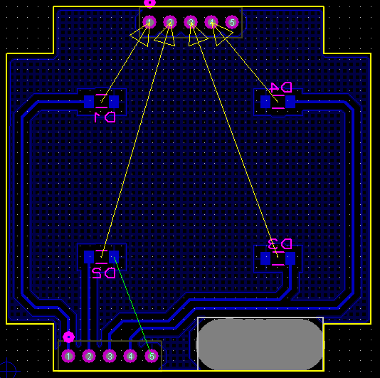
Design description:
1. using CAP touch as single touch button.
2. designed as CAP Addon card which is interface with controller through header pin connector of 2.54mm pitch.
3. the MCU MSP430FR is placed near to connector as to avoid the loop structure or antenna creation.
4. Layout of CAP button:: PAD size - 10mm
:: keepout dist. from PAD to GND - 1mm (recommended)
:: GND plan top layer 75% hatched type and bottom layer 25% hatched type
:: the shape of GND plan to PAD is hexagonal type
:: PAD shape is round
:: PAD is unmasked green open to air
:: NP ohm pull down resistor is connected on signal line from PAD to controller, it is near to MCU
:: we have keept 2mm of through hole in center of PAD for LED indication.
:: signal trace is 12mils(0.3mm).
So, describing these design layout please help us to solve our problem and issues regards the same. Also I have described the doubts and query as we are doing REVISION-2 layout for CAP touch card PCB. So, please do refer and reply as soon as possible as it is very much urgent.
Query and Doubts:
1. what should be the distance between PAD and MCU OR placement of PAD from MCU. It is compulsory for us to design CAP touch as separate PCB only as addon card to controller PCB.
2. should we connect resistor in series from PAD and MCU for ESD protection, as to avoid RF noise nearer. IF yes what should be appropriate value of the resistor. Also where should the resistor be placed, whether near to MCU or PAD.
3. Layout guidance, what should be GND pouring hatched type or 100% filled GND.
4. what should be the size of average PAD for a human touch(recommended 10MM)
5. whether the PAD should be mask with green layer or not
6. what should be the PAD shape for smooth sense.
Kindly help to support so that we can take our product in production.
Thanks in advance
Pradhan