This thread has been locked.

If you have a related question, please click the "Ask a related question" button in the top right corner. The newly created question will be automatically linked to this question.

MSP432P401R: How to route MSP432 with BGA Package

Part Number: MSP432P401R

Hi,

i want to design the MSP432 with BGA Package and want to design the pcb with low cost.

Micro vias and via in pads are expensive and i need to get the route out of the package somehow.

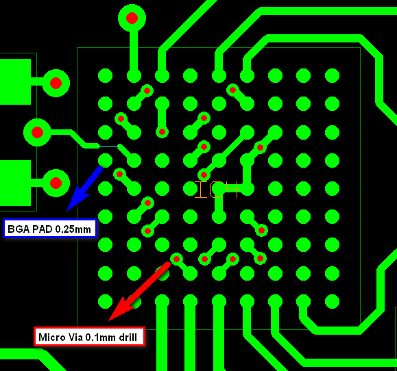
On the datasheet the BGA Pad should have  0.25mm diameter and i design all BGA Pads with 0.25mm.

To avaoid micro vias and make the pcb cheaper, i want to route between the PADs and use normal vias outside the IC.

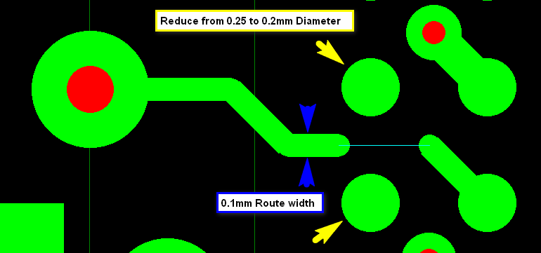
I dont need to route all Balls since i only use a few. My idea was to make some BGA Pads to 0.2mm so i can route with 0.1mm width

and have the pad to route spacing to 0.1mm.

My question is can i reduce Pads that i dont use, that are on the way that i want to route, from 0.25mm to 0.2mm?

The worst case is that the unused ball wont be connected with the 0.2mm PAD right?

But will the other BGA balls be connected?

  • Hello Michael,

    The pad diameter specified is with the tolerance to allow for slight movement during soldering or due to flattening of the pads during soldering. By reducing the size of the pad diameter you are making the design more susceptible to a misconnection due to movement of pad. At a 0.1 mm trace width the cost is already on the higher side. You can avoid using both via on pad and micro via, by following a escape route policy of micro-via between pads which is a more robust and acceptable solution.

  • Hi Amit,

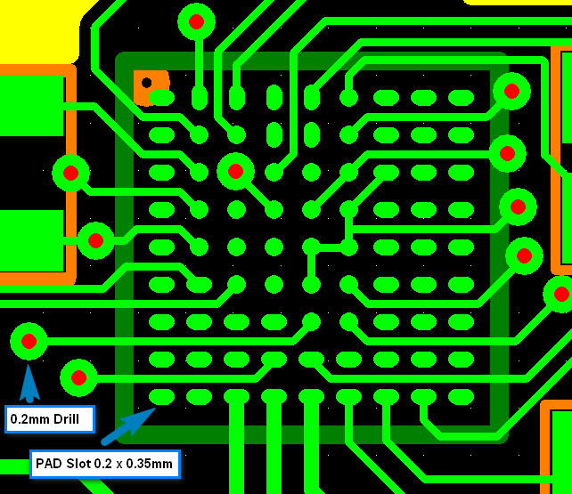
    i change the PAD to 0.2x3.5mm and will try it out.
    The slot area is the same for the solder paste as the circle 0.25mm Pads. The Ball should connect to it.
    This way i can use 0.1mm spacing between Pads and Routes and still use routes as 0.1mm.

    Micro via makes it expensive because the pcb baord should have at least 1mm thickness. Now with normal vias with drills of 0.2mm they can make pcb with normal thickness like 1.5mm

    I will test it and give here a feedback if it works.

  • Hello Michael,

    I would advise you to check with the board assembly house and whether a change of the pad geometry would or would not cause any issues during assembly. If the board house confirms, then it should be OK, but frankly keeping the requirements as given in the datasheet/TRM is the most strongly recommended resolution
  • In my experience, if you want to go low cost, low volume,  then you do not use BGA. As you have seen routing is a pain and board costs could be more for low volume. When you get to high volume I would not worry about it. There is not much cost difference. 

    The other thing is BGA is also harder for hand soldering. You have to use a special machine to hand place it and shoot hot air on it to solder it. When you get above 30 pieces then it is worth a pick-n-place machine. And you do not need 30 for prototypes, so they are hand soldered.  

    I have no idea what your project is or what volume you are talking about. But for me, if I were making less than 1000 I would not use a BGA at all. Keep it simple. 

    Kip

**Attention** This is a public forum