This thread has been locked.

If you have a related question, please click the "Ask a related question" button in the top right corner. The newly created question will be automatically linked to this question.

CCS/MSP430FR6989: I2C transfer between two boards

Part Number: MSP430FR6989
Other Parts Discussed in Thread: ENERGIA, , BOOSTXL-EDUMKII

Tool/software: Code Composer Studio

Hi I am trying to replicate the same scenario as in the previous question. However, as I don't have access to a 10k resistors, are they really necessary? Will it work if I don't make the 10k connections? And also, which jumpers are "eZ-FET lite jumpers" as talked about in the reply that was marked as resolved?

Thanks in advance, 

  • Hi Adwaya,

    yes, the pull-up resistors are definitely necessary.
    The I2C lines are based on open drain drivers. The pull-up pull the lines up to a logic high level, the internal drivers can then force them to a logic low level.
    Do you have access to any other resistors? Might work with something like 4k7 or 6k8 as well.

    The "eZ-FET lite jumpers" are the connectors in the middle of a TI launchpad board. They connect the MSP with the debug module and the power supply from USB. In that post they tried unconnecting one board from USB power supply and then connecting the supply pins of both boards with each other. So one board gets power over USB and "shares" that power with the other board.

    Hope that helps, best regards
    Simon
  • Right now I don't have any resistors. Can the communication between two MSP430 boards be done without resistors using other protocols, such as SPI (I am not too familiar with it but I will look it up if it would work).
  • It should work with SPI, you'll have to define one board as master and one as slave. Just connect the clock and chip select lines with each other and MOSI with MISO.
    There are several code examples from TI which explain the software part pretty good (www.ti.com/.../toolssoftware) or you can use example projects of Energia, if you are using a LaunchPad.

    Otherwise you could try UART, there you have the RX and TX lines which you'll have to cross-connect.
  • Hello Adwaya,
    I need to correct Simon's statement on the pull-ups. The MSP430FR6989 supports the use of the internal Pull-Up/Pull-Down resistors also at the SDA/SCL I2C pins. The reason we do not recommend it, is the value of the resistors, which is not I2C spec compliant, as too high resistance. Thus with higher data rates and higher capacitive loading, this might cause problems with degradation of the I2C signals. With short connections and low speed it should work though.
    A possible workaround would be using the internal resistors at the GPIOs of neighbored pins of SDA/SCL, configuring them as inputs, and activating the pull-up function. This way you can have lower resistance pull-ups without external components. The difficulty might be to generate the connection of those pins with SDA/SCL at the same time, while applying cables at SDA/SCL between the two MSP430 boards.

    So probably the interconnection by SPI or UART is easier. You can find respective code examples in the TI Resource Explorer in CCS.

    Best regards
    Peter
  • The thing is I might end up with a situation that requires multislave single master condition, which, as far as I know, is easy to do with I2C. Will SPI/UART support that as well?
  • Hello Adwaya,
    with UART it will get very difficult or even impossible. UART is not defined for such a use case. With SPI master to multiple slaves is possible "quite" easy.

    Best regards
    Peter
  • Okay: By the way, for I2C, you mentioned "With short connections and low speed it should work though." with the internal high resistance pull-up/pull-down resistors at the SDA/SCL I2C pins. What I am really trying to develop is a simple two-person game which will involve three launchpads (two slaves, one for each user) and a single master launchpad, which will simply show the score (on its LCD screen) based off data from the two slave launchpads. The entire game might run up to two-mins max. The game involves inputs from components such as joystick, accelerometer, buzzer, push-buttons (all on BoosterPacks, one attached to each slave). This might be hard to predict without actually doing it but do you think this scenario is "short connection and low speed" enough?
    Thanks a lot for all your inputs. I just want to make a decision about which communication protocol to finally use that's all.
  • From what you have mentioned, it sounds like your master device will negotiate data from each slave device at certain intervals (I2C is one master to many slaves but not the opposite) . If this is your plan, you should be able to use UART to achieve the same if your master board supports 2 UARTs. All you would need is a 3 wire connection (GND, TX, and RX) between each of the 2 boards to the master. Each connection mus be made at a separate UART of the master.

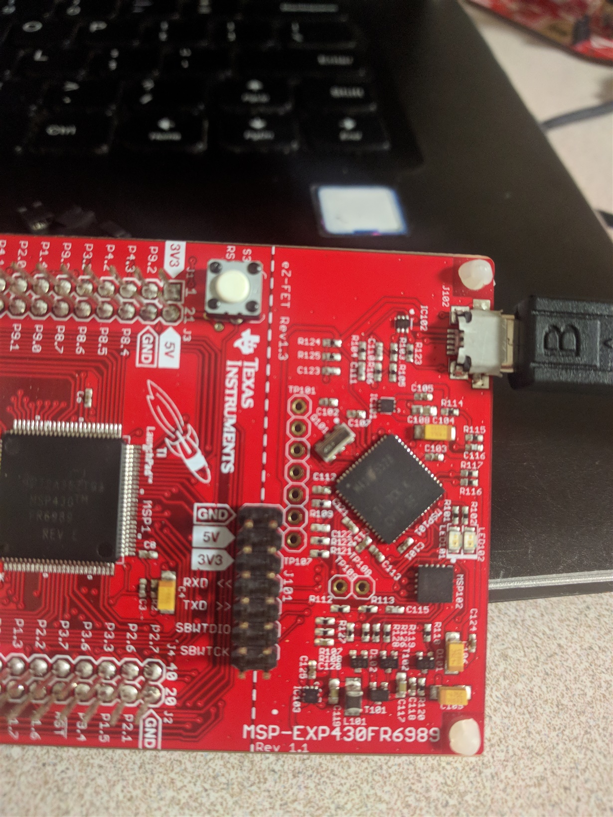
  • Hmm do you mean a connection should be made from each of the slave's GND, TX, and RX pin to the GND, TX, RX pin of the Master respectively? All three boards are MSP430FR6989 by the way. Can this board support two UARTs? This is how it looks like: From the picture, it does look like each board can support two UART connections. Please let me know what you think as I am still trying to decide which one to use before I venture into the coding. Thanks in advance

  • Your board seems to have the 100-pin package. From the datasheet, P2.0 and P2.1 are for UART0 (UCA0RXD and UCA0TXD) and P3.4 and P3.5 and for UART1 (UCA1RXD and UCA1TXD) .
    This means that one of your slave devices will be connected to GND, P2.0, and P2.1. The other slave would be connected to GND, P3.4, and P3.5.
  • Okay I think I have a problem. I am not truly an expert on UART so forgive me if I am being wrong or foolishly obvious. So do you mean the connections should be:

    Slave1 GND ---> Master GND

    Slave1 RXD ---->Master P2.0

    Slave1 TXD ---->Master P2.1

    Slave2 GND ---> Master GND

    Slave2 RXD ---->Master P3.4

    Slave2 TXD ---->Master P3.5

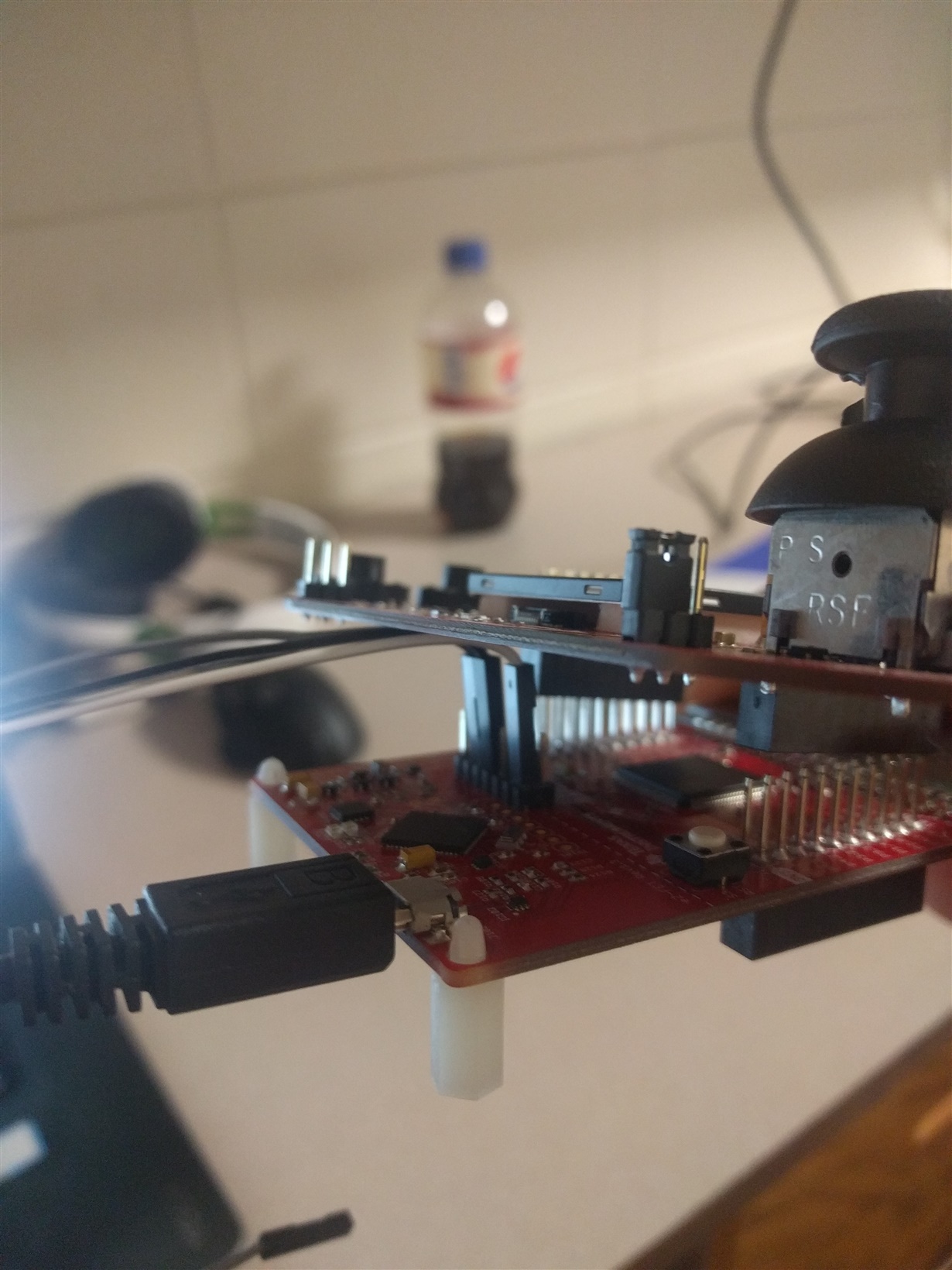
    Because if this is true I will have a problem because the BoosterPack won't fit on the slave if I have wires coming out of its RXDs and TXDs. This is how it looks like if I try to do it:

    Or should it be:

    Slave1 GND ---> Master GND

    Slave1 P2.1 ----> Master P2.0

    Slave1 P2.0 ----> Master P2.1 (This may not be necessary as Master is not transmitting data to slave, isn't it?)

    Slave2GND ----> MasterGND

    Slave2 P2.1 -----> Master P3.4

    Slave2 P2.0 -----> Master P3.5 (Similar question as for Slave 1)

    Finally, I could not find P3.4 and P3.5 on the board can you tell me where they are located exactly?

    Thanks so much for your responses.

  • You wiring scheme is correct. If data receiving is triggered by the master then you need to send a trigger byte from the master. If the data receiving is asynchronous then you are correct, master TX is not needed. But, make sure your master receive ISR is very brief so that you do not lose data do to interrupt priority between UART0 and UART1.
    If P3.4 and P3.5 are not routed to the 2 headers, you will need to somehow make the connection using a soldering iron. You will need it anyways to solder the UART wires directly to overcome the fitting issue.
  • To confirm, the correct one is the one after the picture right?

    And also, it is unlikely I will have access to solder in the immediate future, so as I don't have 10k resistors either, will SPI be the best option for me?

  • No wait. You do have a mistake in wiring after the picture (I am not including GND here, but you should):
    Slave-1 TX0 (P2.0) ----> Master RX0 (P2.1).
    Slave-2 TX0 (P2.0) ----> Master RX1 (P3.5).
  • Okay good. Some last questions. Where is P3.5 located on the board? I scoured through the board and could not find the label P3.5.
    Finally, the master does not have the booster pack on (only the slaves do) so no soldering should be required right? (The booster pack is BOOSTXL-EDUMKII)
  • P3.5 is not connected to a pin header, but to the isolation jumper block and to the eZ-FET Emulator MCU.

    That means that you would have to disconnect the TXD and RXD jumpers of that block to communicate with an other device over UART, but then it's not possible to programm your MSP-Board.

    With this in mind, maybe it's better to try communicating over SPI.

  • Hello Adwaya, Gentlemen,
    there would be a few things to clean up, as e.g. on the second photo the UART cable connections are on the debugger side, thus connected to the PC and not the MSP430 device...
    But I think we need to make a step back here.
    Based on the communication and the photos it looks like you're intending to drive the BOOSTXL-EDUMKII by the FR6989 LaunchPad.
    If this is correct, I see a fundamental problem with this approach, as from the BOOSTXL-EDUMKII you can see two things.
    1. This Boosterpack is designed for the MSP432 Launchpad and not for the MSP430FR6989.
    2. The Boosterpack comes without its own MCU, means all the functionality to operate it needs to come from the connected LaunchPad.

    Derived from this, you would need to convert the code from MSP432 to MSP430. While in theory this might be possible, irrespective of the effort, you need to consider the HW, at first point the interconnections between the LP and the BP. These are designed on the BP side for the MSP432 LP, means will probably at many spots not fit the connections and functionality on the MSP430FR6989 side. There are a lot of sensors and control elements on the BP side, analog sensors, which require ADC functionality at certain pins, and digital sensors, requiring I2C communication. Means quite some communication resources on the LP side will already be occupied by these, and even these should be available at the right pins of the LP, they are occupied by the BP, means you cannot use them for interconnections to the other LPs.
    Thus I would recommend making a step back, and reconsidering the use of the LP for the BP, but first checking with the tool's documentation, what physical interconnection and resources are available for the desired setup and functionality at all.

    Best regards
    Peter
  • Hello Peter,
    Yeah you are right the wires in the second picture do need to be connected to the MCU side not the PC my bad.

    However, I have been using/setting up various components of the BOOSTXL-EDUMKII using the MSP430FR6989 for weeks now (the accelerometer, joystick, buttons, LEDs etc..). So the conversion from MSP432 to MSP430 is no longer an issue I think.

    But to set up UART, if I configure the P2.0 (UCA0TXD) and P2.1(UCA0RXD) on each slave (albeit with the BoosterPack connected on top of it),I should still be able those pins normally as I am not using them for anything else (in the BoosterPack, I am only using Joystick, Acceleromter, Buzzer, LEDs, pushButtons) and the functionality at the pins can be determined by setting the PxSEL bits. As I only want to use the UART of the Launchpad, I should be able to connect the three boards, without taking into account that two of them have BoosterPacks attached to them, shouldn't I?
  • Hello Adwaya,
    understood.
    So in terms of the P2.0/P2.1, you would need to check whether there is something conflicting in HW with BP, means something which would corrupt the signals. From the documentation I can see on the BP P2.1 goes to PWM Servo. So if you have nothing connected there, this should be fine. With P2.0, there is an ambient light sensor output with pull-up on this connection. The pull-up might indicate it is an open drain output. In any case you need to make sure the light sensor doe not pull the signal low, or drive a high actively, if it's not an open drain.
    On the FR6989 side I could not see anything critical.

    Best regards
    Peter
  • Hello Peter,
    Hmm that is indeed a valid concern regarding (P2.0) . Looking at the Pinout Diagram for the BP, I am not entirely sure how it would the signals would come out if I set the UCA0TXD on P2.0 . Since the light sensor would require I2C input set up for the two pins below it (P4.1 and P4.0) I am guessing the functionality for the light sensor would be incomplete for the light sensor if I don't set up I2C for it shouldn't it? (which means I would be able to use P2.0 normally as if on the LP?)

    Are there any other ways around this problem (if it is a problem)? (My only concern is achieving the communication, I don't really care if I use UART or SPI). Simon here suggested using SPI but even if I decide to use SPI, I would still need to use P2.0 and P2.1 (or P4.1 and P4.2), which gives rise to the same problem.
  • Hello Adwaya,
    I checked the datasheet of the light sensor and I think you should not have an issue with it. On one hand the INT output is an open drain, this means it would only in case of interrupt condition pull the signal low. But this should not happen, because according to the device, the device starts up in a low-power shut down state. Thus without any configuration through the I2C, the device should not generate any INT events, and thus never pull down the INT signal. The pull-up is no issue for the UART communication. The MSP430 GPIOs can drive this without problems. Of course the pull-up will cause some additional current. So for best ULP performance it would make sense to remove the pull-up, but for the UART functionality it will be not an issue.
    So if for the two slave LPs you can use two separate UART connections to the master. This should be fine.

    Best regards
    Peter
  • Thanks a lot that's a relief. So how do we make two connections in the master? I found this code in TI Resource Explorer (included below), which sets up one UART. How do we set up the second UART in the code for MASTER? (syntax...)

    ; --/COPYRIGHT--
    ;******************************************************************************
    ;  MSP430FR69xx Demo - USCI_A0 External Loopback test @ 115200 baud
    ;
    ;  Description: This demo connects TX to RX of the MSP430 UART
    ;  The example code shows proper initialization of registers
    ;  and interrupts to receive and transmit data. If data is incorrect P1.0 LED is
    ;  turned ON.
    ;  ACLK = n/a, MCLK = SMCLK = BRCLK = default DCO = 1MHz
    ;
    ;
    ;                MSP430FR6989
    ;             -----------------
    ;       RST -|     P2.0/UCA0TXD|----|
    ;            |                 |    |
    ;            |                 |    |
    ;            |     P2.1/UCA0RXD|----|
    ;            |                 |
    ;            |             P1.0|---> LED
    ;
    ;   E. Chen
    ;   Texas Instruments Inc.
    ;   April 2014
    ;   Built with Code Composer Studio V6.0
    ;******************************************************************************
    ;-------------------------------------------------------------------------------
                .cdecls C,LIST,"msp430.h"       ; Include device header file
    ;-------------------------------------------------------------------------------
                .def    RESET                   ; Export program entry-point to
                                                ; make it known to linker.
    ;-------------------------------------------------------------------------------
    RXData      .set    R5
    TXData      .set    R6
    ;-------------------------------------------------------------------------------
                .global _main
                .global __STACK_END
                .sect   .stack                  ; Make stack linker segment ?known?
    
                .text                           ; Assemble to Flash memory
                .retain                         ; Ensure current section gets linked
                .retainrefs
    
    _main
    RESET       mov.w   #__STACK_END,SP         ; Initialize stackpointer
    StopWDT     mov.w   #WDTPW+WDTHOLD,&WDTCTL  ; Stop watchdog timer
    SetupGPIO   bic.b   #BIT0,&P1OUT            ; Clear P1.0 output latch
                bis.b   #BIT0,&P1DIR            ; For LED on P1.0
                bis.b   #BIT0+BIT1,&P2SEL0      ; USCI_A0 UART operation
                bic.b   #BIT0+BIT1,&P2SEL1
    
    UnlockGPIO  bic.w   #LOCKLPM5,&PM5CTL0      ; Disable the GPIO power-on default
                                                ; high-impedance mode to activate
                                                ; previously configured port settings
    
    SetupUART   mov.w   #UCSWRST,&UCA0CTLW0     ; Put eUSCI in reset
                bis.w   #UCSSEL__SMCLK,&UCA0CTLW0 ; CLK = SMCLK
                mov.b   #8, &UCA0BR0            ; 1000000/115200 = 8.68
                bis.w   #0xD600,&UCA0MCTLW      ; 1000000/115200 - INT(1000000/115200)=0.68
                                                ; UCBRSx value = 0xD6 (See UG)
                clr.b   &UCA0BR1
                bic.b   #UCSWRST,&UCA0CTL1      ; release from reset
                bis.w   #UCRXIE,&UCA0IE         ; Enable USCI_A0 RX interrupt
                mov.w   #0,RXData               ; RXData = 0
                mov.w   #1,TXData               ; TXData = 1
    
    Mainloop    bit.w   #UCTXIFG,&UCA0IFG
                jeq     Mainloop
                mov.w   TXData,&UCA0TXBUF       ; Load data onto buffer
                nop                             ;
                bis.w   #LPM0+GIE,SR            ; Enter LPM0, interrupts enabled
                nop                             ; For debugger
                jmp     Mainloop
    
    ;------------------------------------------------------------------------------
    USCI_A0_ISR;    USCI A0 Receive/Transmit Interrupt Service Routine
    ;------------------------------------------------------------------------------
                add.w   &UCA0IV,PC              ; add offset to PC
                reti                            ; Vector 0: No interrupts
                jmp     Receive                 ; Vector 2: USCI UCRXIFG
                reti                            ; Vector 4: USCI UCTXIFG
                reti                            ; Vector 6: USCI UCSTTIFG
                reti                            ; Vector 8: USCI UCTXCPTIFG
    Receive     mov.w   &UCA0RXBUF,RXData       ; Read buffer
                cmp.b   RXData,TXData           ; Check value
                jne     LEDOn
                inc.w   TXData                  ; increment data byte
                bic.w   #LPM0,0(SP)             ; Exit LPM0 on reti
                reti
    LEDOn       bis.b   #BIT0,&P1OUT            ; If incorrect turn on P1.0
    TrapCPU     jmp     TrapCPU                 ; Trap CPU
                reti
    ;------------------------------------------------------------------------------
    ;           Interrupt Vectors
    ;------------------------------------------------------------------------------
                .sect   ".reset"                ; MSP430 RESET Vector
                .short  RESET                   ;
                .sect   USCI_A0_VECTOR          ; USCI A0 Receive/Transmit Vector
                .short  USCI_A0_ISR
                .end
    

  • Adwaya,
    the approach is pretty simple. The MSP430FR6989 has two UARTS, eUSCI_A0 and eUSCI_A1. These blocks are completely equvalent, so configuration, control registers, performance is the same. The difference is the index in the register name, and of course the physical pins.
    So to modify this code example from USCI_A0 to USCI_A1 you just need to replace everywhere the A0 by A1, and instead, or better to say in addition of selecting the UART function for P2.0 and P2.1, you need to select it also for USCI_A1. There would be two options from the FR6989 device, but the one is occupied by connections to LCD segments. It would be possible to run the UART communication on these with connected LCD segments, but over time this would damage the LCD, thus the P3.4, P3.5 option is the better one. But you of course need to disconnect the jumpers to the virtual COM port of the debugger section.

    Best regards
    Peter
  • Hello Peter,
    Thanks for that I was thinking it would be like that. Would you be kind enough to go to the link Bruce McKenney gave before your most recent post and check out how I wrote my MASTER CODE (and see if that's what you mean?).

    Thanks a lot for your help and advice.
  • Hello Adwaya,
    in principle this should work, but it is a bit dangerous to rely on the response from the slave at the master.
    The point I am trying to make, as far as I could see from your code, you have just the UART RX interrupt enabled. This means you're transmitting a byte to the slave, then go to sleep. If for whatever reason the slave should not respond, you're stuck for ever in LPM. So maybe it would make sense having a Timer interrupt running in the background, which would save you in this case on the master side, wake you up after a timeout, and you could try re-sending data to the slave.

    Best regards
    Peter
  • Hello Peter,
    Okay I am trying to set-up the UART and I am kinda stymied by the logistics of doing it. So both the slave code and the master code should be in the same project? And should I upload the master code and the slave code separately to each launchpad and then have the slave plugged in while running the code?
    Oh by the way, how do you create a new .asm file in a project?
    Thanks,
    Adwaya
  • Hello Adwaya,
    please let me outline, how I would set up the communication, based on my understanding of the functionality you're trying to achieve.
    First let me rephrase what I have understood, just to make sure, we're on the same page.
    So as far my understanding goes, you want to have one master, which will be connected to two other LPs used as slaves. We have decided to do these connections by UART communication.
    Now as the UART protocol and HW as such doesn't cover master-multi-slave communication, the suggestion was to use point to point connections from the master to the two slave LPs. This can be done by using two separate UART channels. One between master and slave 1 and the other from master to slave 2.
    Derived from this the following further suggestions on the outline of code can be made:
    1. The master needs to have 2 UART RX and TX functions for the two UART channels.
    2. Each slave needs to have 1 UART RX and TX function for the communication with the master.
    3. The functions, determining or implementing the master/slave functionality need to happen on higher SW levels. This means, usually in a master slave system, the master is the one who triggers communication. This means the slaves would be waiting with active UART RX interrupt on the master triggering by a UART communication, transmitting either data or instructions, to respond accordingly. either by setting respective activities or providing requested information to the master.
    4. Thus the low level initialization for the UART would be the same on both slaves.
    5. Even the initialization of the master's UARTs would be the same as on the slave side, as the RX interrupt can be enabled also on the master side.
    6. You need to define some kind of a simple protocol for the communication, to address synchronization and data integrity checks. It could be e.g. something like this:
    bytes
    - 1. 2. synchronization pattern (usually 0xAA and 0x55)
    - 3. number of transmitted bytes
    - 4. data transmitted (instructions/data)
    - 5. Checksum
    The assignment of the functionality to the transmitted bytes happens on a higher level of the code.

    The assignment/trigger of the activities derived from the communication content happens then on even higher SW layers.

    The code for the master and the slaves would be two separate projects.
    I hope this clarifies it a bit more.

    Generating a new source file is simple. Go to pull down menu File >> New >> Source File. In the menu, which opens at that point you can define, whether it should be a .c or .asm file.

    Best regards
    Peter
  • Peter,
    Thanks a lot for that it really helped with the setup. I don't understand the part about data synchronization though. So part of my game involves checking which slave finished the game first, (to give bonus points to whichever slave finished first). Right now, although the two UART channels seem to be working perfectly during the game, as soon as I try to compare who finished first in the end, it returns unexpected results. Either the score would be calculated wrong in the end, or the information would not be transmitted in the end or both. As each slave does not know the condition of the other slave, the master transmits to each slave what the other slave is doing, so that each slave could figure out whether it has won the game or not. 
    I have posted details about the problem in my question in:

    e2e.ti.com/.../749893


    This is basically the last hurdle in my project. As soon as I deal with this, I will be done!

    Regards,
    Adwaya

  • Hello Adwaya,
    not sure, what you mean in the other thread with supplying one of the boards by 5V. Just in case, please keep in mind the supply voltage limits of the MSP430.
    Regarding synchronization, the point with a UART protocol and others is, you should always keep in mind the scenario of missing the start of a communication packet. So to be able to recognize the start of a protocol, you need to use some kind of a recognizable marker, each packet would start with. That is with wired communication protocols usually the 0xAA 0X55 pattern.
    In terms of your problem, I would recommend a different approach. As the master is receiving the information from the slaves, I would let the master decide, who is the winner. You could have an "RTC" running on the master side, adding a time stamp to the received packets from the slaves. Once a slave would send the message game completed, you would based on the time point of reception on the master side assign a time stamp to it. In the end you can compare when the "game completed" messages from the slave occurred, and communicate accordingly to the slaves the winner/looser message. Or you could send in the occurrence of the first "game completed" message to its transmitter the winner message and to the other one "game lost " message.
    I am not sure how long your UART protocol and the baud rate is, but one potential failure case might be missing a UART RX interrupt to too long engagement in the ISR for the other UART. Thus the recommendation to keep the ISR as short as possible. Just pushing the received data into RAM, and flagging the reception. Processing should happen outside the ISR at a later point.

    As you're discussing the problems also in the other thread you've opened, please close this one. Many thanks in advance.

    Best regards
    Peter
  • Righto I will do that and post further questions in that post. Thanks to all of you who participated in this discussion.
    Thanks,
    Adwaya
  • Hello Adwaya,
    many thanks, though you made a small mistake on the thread closure. This is related to our E2E system setup. In case you would like to post a final comment, you need to do this first, and then click on "resolved..". Otherwise any additional post will keep the thread open, as it is now.
    Just to keep in mind in the future, I'll close it now.
    A lot of success with your project!

    Best regards
    Peter

**Attention** This is a public forum