This thread has been locked.

If you have a related question, please click the "Ask a related question" button in the top right corner. The newly created question will be automatically linked to this question.

MSP430F5438A-EP: MSP430F5438A as SPI slave

Part Number: MSP430F5438A-EP
Other Parts Discussed in Thread: MSP430WARE, MSP430F5438A,

Hi,

I would like to take the discussion further where I left last time. Please look at my previous post which was almost 9 months back.

https://e2e.ti.com/support/microcontrollers/msp430/f/166/t/766491

Now, I am using FPGA between my Communication Transceiver and MSP430.

FPGA will constantly receive DATA and CLK from the Communication Transceiver and look for a pattern of DATA sampled at the CLK provided by the communication transceiver. This pattern of data we call as start of frame (SOF). Once it receives SOF, it will set one of its pin as chip select (CS active high) to high and forward the CLK, DATA and CS to MSP430 SPI slave. We have a pattern of data for end of frame as well (EOF). And once FPGA sees the EOF, it will deselect the MSP430 SPI slave by setting the CS as low.

When I tried to run my system and receive, my MSP430 sometimes receives the DATA properly and sometimes DATA shifted by few bits (around 1-4 bits).

I realised that my CS was getting activated at the same edge of the CLK where DATA is to be sampled.

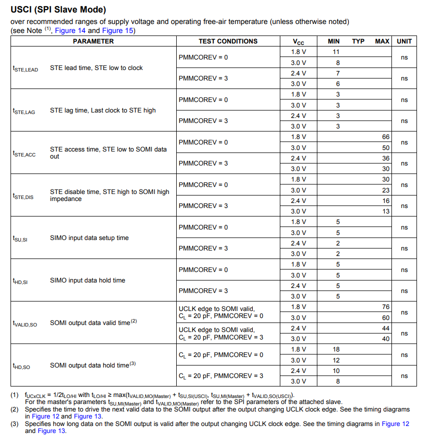
Now it seems like I am kind of creating my own SPI master using FPGA. That means I need to handle the timing constraints as mentioned below:

So my CS should come at least 11 ns earlier. I plan to put CS high around CLK/4 time earlier than the next CLK and DATA. Would that be OK?

Can anything else also cause the bit shift issue? Also do let me know if I have to handle something else as well.

I would like to know how SPI slave triggers an interrupt for receive. Does it trigger based on 8 input SPI CLK after the SPI is enabled? 

My ISR looks like below (used reference from SPI slave MSP430F5438A example from MSP430ware) :

#define SLAVE_CS_IN P3IN
#define SLAVE_CS_DIR P3DIR
#define SLAVE_CS_PIN BIT0

void USCI_B0_ISR (void)

{
switch (__even_in_range(UCB0IV,4)){
//Vector 2 - RXIFG
case 2:
if(SLAVE_CS_IN & SLAVE_CS_PIN)
receiveData[cnt++] = UCB0RXBUF;
break;

default: break;
}
}

Thanks and Regards,

Ankit

  • Hello Ankit,

    Let me address your questions here:

    So my CS should come at least 11 ns earlier. I plan to put CS high around CLK/4 time earlier than the next CLK and DATA. Would that be OK?
    [I don't know what your clock rate is so I would leave adequate time and following the diagram and timing specifications in the datasheet.]

    I would like to know how SPI slave triggers an interrupt for receive. Does it trigger based on 8 input SPI CLK after the SPI is enabled?
    [Yes. It is described in the MSP430x5xx_x6xx user guide, starting in section 37.2.  You might also want to check out the SPI examples for this device in the TI resource explorer.  Look in the Software folder for MSP430Ware-3.80.07.00 , then Devices, then MSP430F5XX_6XX folder.  There several SPI examples that will show you the proper method to configure the SPI and respond to interrupts.]

    Can anything else also cause the bit shift issue? Also do let me know if I have to handle something else as well.
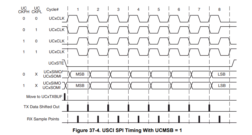
    [Generally this is caused when the serial clock polarity and phase are not configured properly between the master and slave.  Refer to section 37.2]

  • Hi Dennis,

    Thanks for your reply. My CLK is 128 KHz. I have set my SPI with CLK PHASE 0 and CLK PLOARITY 1.

    I am attaching the waveforms taken from oscilloscope of my SPI signals.

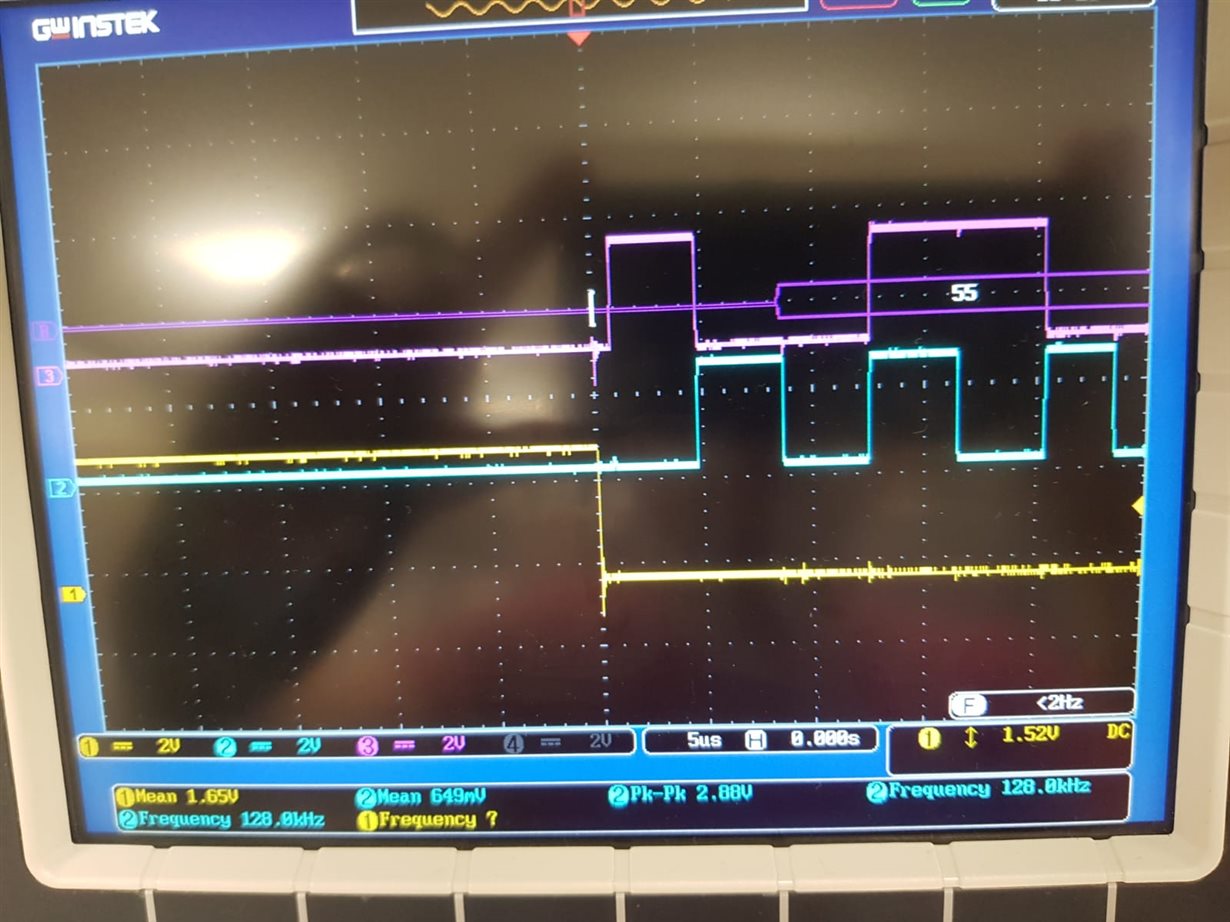
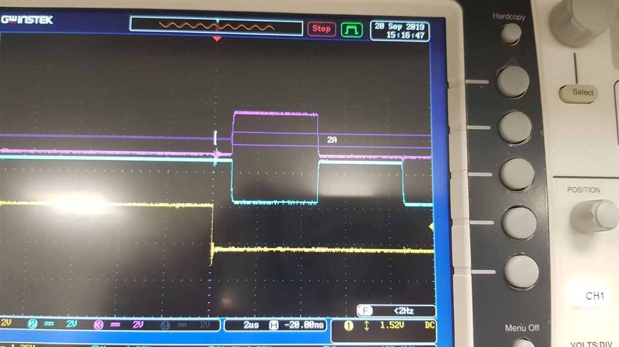
    Note: Yellow is CS (I changed to Active Low). Blue is CLK. Pink is DATA.

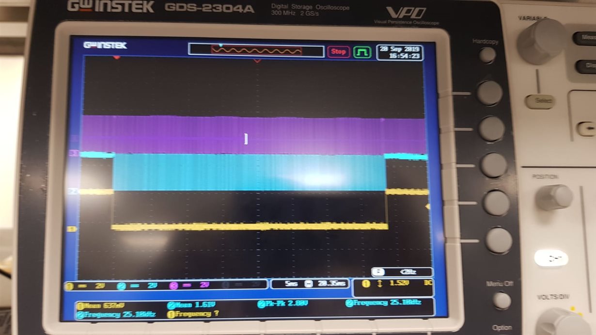
    This is one full transaction:

    Below is the image where CS (changed to active low) is asserted. Here I think I can safely assume that tSTE_LEAD is safely above 11ns mentioned in datasheet. It is around 400ns.

    My CS is de-asserted in the image below. tSTE_LAG is supposed to be minimum 3 ns. We are giving around 1.6 us.

    So, I am using SPI in 3 wire slave mode by initializing as below:

    void InitializeUcb0(void)
    {
        //P3.2 UCB0SOMI as output
        GPIO_setAsPeripheralModuleFunctionOutputPin((uint8_t) GPIO_PORT_P3,
                                                   (uint16_t) GPIO_PIN2);
        //P3.3 UCB0CLK, P3.0 UCB0STE and P3.1 UCB0SIMO as inputs
        GPIO_setAsPeripheralModuleFunctionInputPin(
                (uint8_t) GPIO_PORT_P3,
                ((uint16_t) GPIO_PIN3));
    
        P3SEL |= 0x01;
    
    /*    GPIO_setAsPeripheralModuleFunctionInputPin(
                (uint8_t) GPIO_PORT_P3,
                ((uint16_t) GPIO_PIN0));*/
    
        GPIO_setAsPeripheralModuleFunctionInputPin(
                (uint8_t) GPIO_PORT_P3,
                ((uint16_t) GPIO_PIN1));
    
        if (STATUS_SUCCEEDED == USCI_B_SPI_initSlave((uint16_t) USCI_B0_BASE, USCI_B_SPI_MSB_FIRST, 0, 1))
        {
    //        SLAVE_CS_DIR &= ~(SLAVE_CS_PIN);
            enable_SPIA();
            //Enable SPI module
    //        USCI_B_SPI_enable((uint16_t) USCI_B0_BASE); //enable the SPI when data is detected on S-Band
            //Enable Receive interrupt
        }
    }


    MY SPI Enable and Disable functions:
    void enable_SPIA(void)
    {
        USCI_B_SPI_enable((uint16_t) USCI_B0_BASE);
        USCI_B_SPI_clearInterrupt(USCI_B0_BASE,
            USCI_B_SPI_RECEIVE_INTERRUPT
            );
        USCI_B_SPI_enableInterrupt(USCI_B0_BASE,
            USCI_B_SPI_RECEIVE_INTERRUPT
            );
    }
    
    void disable_SPIA(void)
    {
        USCI_B_SPI_disable((uint16_t) USCI_B0_BASE);
    }


    My CS, I have chosen as interrupt pin P 1.6
        P1DIR &= (CLR_SEVENTH_BIT & CLR_EIGHTH_BIT);
    //    P1IES |= SET_SEVENTH_BIT /*| SET_EIGHTH_BIT*/;
        P1IES &= CLR_SEVENTH_BIT;
        P1IE |= SET_SEVENTH_BIT /*| SET_EIGHTH_BIT*/;
        P1SEL &= (CLR_SEVENTH_BIT & CLR_EIGHTH_BIT);
    
    void PORT1_ISR(void) __attribute__((interrupt(PORT1_VECTOR)));
    void PORT1_ISR(void)
    {
        switch (__even_in_range(P1IV, (uint16_t)0x0E))
        {
        case P1IV_P1IFG1:
            (*regCallback2)();
            break;
        case P1IV_P1IFG6:
            (*regCallback1)();
            break;
        default:
            break;
        }
    }


    the regCallback1 is actually a printing task which will throw all the received SPI data over UART to Serial Terminal.

    void print_app(void)
    {
    //    sprintf(printArr, "CIM Print App %lu!\n\r", counter);
    //    UART0_Put_Chars((uint8_t*)printArr, strlen(printArr));
    //    counter++;
    //    P1OUT ^= 0x01;
    //    if(505 == cnt)
            disable_SPIA();
            P1OUT ^= 0x01;
            UART0_Put_Chars((uint8_t*)receiveData, cnt);
            cnt = 0; //todo need to check the race condition
            enable_SPIA();
    }


    MY SPI ISR is below:

    #define SLAVE_CS_IN     P1IN
    #define SLAVE_CS_DIR    P1DIR
    #define SLAVE_CS_PIN    BIT6
    
    //******************************************************************************
    //
    //This is the USCI_B0 interrupt vector service routine.
    //
    //******************************************************************************
    #if defined(__TI_COMPILER_VERSION__) || defined(__IAR_SYSTEMS_ICC__)
    #pragma vector=USCI_B0_VECTOR
    __interrupt
    #elif defined(__GNUC__)
    __attribute__((interrupt(USCI_B0_VECTOR)))
    #endif
    void USCI_B0_ISR (void)
    {
        switch (__even_in_range(UCB0IV,4)){
            //Vector 2 - RXIFG
            case 2:
                if(!(SLAVE_CS_IN & SLAVE_CS_PIN))
                    receiveData[cnt++] = UCB0RXBUF;
                break;
    
            default: break;
        }
    }

    Now the problem that I am facing is, my SPI ISR doesn't work when I comment "P3SEL |= 0x01" in InitializeUcb0; which is actually STE pin for UCB0 SPI. And I am not able to understand what STE pin has to do with SPI slave setting when I am using 3 wire SPI slave mode. As soon as my UCB0 module receives consecutive 8 SPI CLK from Master, it should hit the SPI ISR irrespective of whether STE is activated or not.

    Please do tell me if you find any other weaknesses in the code.


    Thanks and Regards,

    Ankit

  • Just to add few more results based on my observation:

    My communication transceiver is sending the following to MSP430 slave periodically:

    Number of characters 624.

    AA AA AA AA AA AA AA AA AA AA AA AA AA AA AA AA AA AA AA AA AA AA AA AA
    AA AA AA AA AA AA AA AA AA AA AA AA AA AA AA AA AA AA AA AA AA AA AA AA
    AA AA AA AA AA AA AA AA AA AA AA AA AA AA AA AA AA AA AA AA AA AA AA AA
    AA AA AA AA AA AA AA AA AA AA AA AA AA AA AA AA AA AA AA AA AA AA AA AA
    AA AA AA AA AA AA AA AA AA AA AA AA AA AA AA AA AA AA AA AA AA AA AA AA
    AA AA AA AA AA AA AA AA AA AA AA AA AA AA AA AA AA AA AA AA AA AA AA AA
    AA AA AA AA AA AA AA AA AA AA AA AA AA AA AA AA AA AA AA AA AA AA AA AA
    AA AA AA AA AA AA AA AA AA AA AA AA AA AA AA AA AA AA AA AA AA AA AA AA
    AA AA AA AA AA AA AA AA AA AA AA AA AA AA AA AA AA AA AA AA AA AA AA AA
    AA AA AA AA AA AA AA AA AA AA AA AA AA AA AA AA AA AA AA AA AA AA AA AA
    AA AA AA AA AA AA AA AA AA AA AA AA AA AA AA AA AA AA AA AA AA AA AA AA
    AA AA AA AA AA AA AA AA AA AA AA AA AA AA AA AA AA AA AA AA AA AA AA AA
    AA AA AA AA AA AA AA AA AA AA AA AA AA AA AA AA AA AA AA AA AA AA AA AA
    AA AA AA AA AA AA AA AA AA AA AA AA AA AA AA AA AA AA AA AA AA AA AA AA
    AA AA AA AA AA AA AA AA AA AA AA AA AA AA AA AA AA AA AA AA AA AA AA AA
    AA AA AA AA AA AA AA AA AA AA AA AA AA AA AA AA AA AA AA AA AA AA AA AA
    AA AA AA AA AA AA AA AA AA AA AA AA AA AA AA AA AA AA AA AA AA AA AA AA
    AA AA AA AA AA AA AA AA AA AA AA AA AA AA AA AA AA AA AA AA AA AA AA AA
    AA AA AA AA AA AA AA AA AA AA AA AA AA AA AA AA AA AA AA AA AA AA AA AA
    AA AA AA AA AA AA AA AA AA AA AA AA AA AA AA AA AA AA AA AA AA AA AA AA
    AA AA AA AA AA AA AA AA AA AA AA AA AA AA AA AA AA AA AA AA AA AA AA AA
    AA AA AA AA AA AA AA AA AA AA AA AA AA AA AA AA AA AA AA AA AA AA AA AA
    AA AA AA AA AA AA AA AA AA AA AA AA AA AA AA AA AA AA AA AA AA AA AA AA
    AA AA AA AA AA AA AA AA AA AA AA AA AA AA AA AA AA AA AA AA AA AA AA AA
    AA AA AA AA AA AA AA AA AA AA AA AA AA AA AA AA AA AA AA AA AA AA AA AA
    AA AA AA AA AA AA AA AA AA AA AA AA AA AA AA AA AA AA AA 1F 32 54 76 F8

    but at MSP430 slave side, sometimes I am receiving the following consistently (thrown by MSP430 slave  through UART at the serial terminal):

    Number of characters 623 (1 character less than the correct version). Looks like 7 bits right shifted version of correct version.

    55 55 55 55 55 55 55 55 55 55 55 55 55 55 55 55 55 55 55 55 55 55 55 55
    55 55 55 55 55 55 55 55 55 55 55 55 55 55 55 55 55 55 55 55 55 55 55 55
    55 55 55 55 55 55 55 55 55 55 55 55 55 55 55 55 55 55 55 55 55 55 55 55
    55 55 55 55 55 55 55 55 55 55 55 55 55 55 55 55 55 55 55 55 55 55 55 55
    55 55 55 55 55 55 55 55 55 55 55 55 55 55 55 55 55 55 55 55 55 55 55 55
    55 55 55 55 55 55 55 55 55 55 55 55 55 55 55 55 55 55 55 55 55 55 55 55
    55 55 55 55 55 55 55 55 55 55 55 55 55 55 55 55 55 55 55 55 55 55 55 55
    55 55 55 55 55 55 55 55 55 55 55 55 55 55 55 55 55 55 55 55 55 55 55 55
    55 55 55 55 55 55 55 55 55 55 55 55 55 55 55 55 55 55 55 55 55 55 55 55
    55 55 55 55 55 55 55 55 55 55 55 55 55 55 55 55 55 55 55 55 55 55 55 55
    55 55 55 55 55 55 55 55 55 55 55 55 55 55 55 55 55 55 55 55 55 55 55 55
    55 55 55 55 55 55 55 55 55 55 55 55 55 55 55 55 55 55 55 55 55 55 55 55
    55 55 55 55 55 55 55 55 55 55 55 55 55 55 55 55 55 55 55 55 55 55 55 55
    55 55 55 55 55 55 55 55 55 55 55 55 55 55 55 55 55 55 55 55 55 55 55 55
    55 55 55 55 55 55 55 55 55 55 55 55 55 55 55 55 55 55 55 55 55 55 55 55
    55 55 55 55 55 55 55 55 55 55 55 55 55 55 55 55 55 55 55 55 55 55 55 55
    55 55 55 55 55 55 55 55 55 55 55 55 55 55 55 55 55 55 55 55 55 55 55 55
    55 55 55 55 55 55 55 55 55 55 55 55 55 55 55 55 55 55 55 55 55 55 55 55
    55 55 55 55 55 55 55 55 55 55 55 55 55 55 55 55 55 55 55 55 55 55 55 55
    55 55 55 55 55 55 55 55 55 55 55 55 55 55 55 55 55 55 55 55 55 55 55 55
    55 55 55 55 55 55 55 55 55 55 55 55 55 55 55 55 55 55 55 55 55 55 55 55
    55 55 55 55 55 55 55 55 55 55 55 55 55 55 55 55 55 55 55 55 55 55 55 55
    55 55 55 55 55 55 55 55 55 55 55 55 55 55 55 55 55 55 55 55 55 55 55 55
    55 55 55 55 55 55 55 55 55 55 55 55 55 55 55 55 55 55 55 55 55 55 55 55
    55 55 55 55 55 55 55 55 55 55 55 55 55 55 55 55 55 55 55 55 55 55 55 55
    55 55 55 55 55 55 55 55 55 55 55 55 55 55 55 55 55 55 54 3E 64 A8 ED

    and sometimes following consistently (thrown by MSP430 slave  through UART at the serial terminal):

    Number of characters 624. Looks like 1 bit right shifted version of correct version.

    55 55 55 55 55 55 55 55 55 55 55 55 55 55 55 55 55 55 55 55 55 55 55 55
    55 55 55 55 55 55 55 55 55 55 55 55 55 55 55 55 55 55 55 55 55 55 55 55
    55 55 55 55 55 55 55 55 55 55 55 55 55 55 55 55 55 55 55 55 55 55 55 55
    55 55 55 55 55 55 55 55 55 55 55 55 55 55 55 55 55 55 55 55 55 55 55 55
    55 55 55 55 55 55 55 55 55 55 55 55 55 55 55 55 55 55 55 55 55 55 55 55
    55 55 55 55 55 55 55 55 55 55 55 55 55 55 55 55 55 55 55 55 55 55 55 55
    55 55 55 55 55 55 55 55 55 55 55 55 55 55 55 55 55 55 55 55 55 55 55 55
    55 55 55 55 55 55 55 55 55 55 55 55 55 55 55 55 55 55 55 55 55 55 55 55
    55 55 55 55 55 55 55 55 55 55 55 55 55 55 55 55 55 55 55 55 55 55 55 55
    55 55 55 55 55 55 55 55 55 55 55 55 55 55 55 55 55 55 55 55 55 55 55 55
    55 55 55 55 55 55 55 55 55 55 55 55 55 55 55 55 55 55 55 55 55 55 55 55
    55 55 55 55 55 55 55 55 55 55 55 55 55 55 55 55 55 55 55 55 55 55 55 55
    55 55 55 55 55 55 55 55 55 55 55 55 55 55 55 55 55 55 55 55 55 55 55 55
    55 55 55 55 55 55 55 55 55 55 55 55 55 55 55 55 55 55 55 55 55 55 55 55
    55 55 55 55 55 55 55 55 55 55 55 55 55 55 55 55 55 55 55 55 55 55 55 55
    55 55 55 55 55 55 55 55 55 55 55 55 55 55 55 55 55 55 55 55 55 55 55 55
    55 55 55 55 55 55 55 55 55 55 55 55 55 55 55 55 55 55 55 55 55 55 55 55
    55 55 55 55 55 55 55 55 55 55 55 55 55 55 55 55 55 55 55 55 55 55 55 55
    55 55 55 55 55 55 55 55 55 55 55 55 55 55 55 55 55 55 55 55 55 55 55 55
    55 55 55 55 55 55 55 55 55 55 55 55 55 55 55 55 55 55 55 55 55 55 55 55
    55 55 55 55 55 55 55 55 55 55 55 55 55 55 55 55 55 55 55 55 55 55 55 55
    55 55 55 55 55 55 55 55 55 55 55 55 55 55 55 55 55 55 55 55 55 55 55 55
    55 55 55 55 55 55 55 55 55 55 55 55 55 55 55 55 55 55 55 55 55 55 55 55
    55 55 55 55 55 55 55 55 55 55 55 55 55 55 55 55 55 55 55 55 55 55 55 55
    55 55 55 55 55 55 55 55 55 55 55 55 55 55 55 55 55 55 55 55 55 55 55 55
    55 55 55 55 55 55 55 55 55 55 55 55 55 55 55 55 55 55 55 0F 99 2A 3B 7C

    If I reset the MSP430, then subsequent results become consistently OK.

    Now clearly there is bit shift involved, however in first wrong case I receive 1 less character but in the second wrong case I receive correct amount of characters. 

    When I try to check the SPI waveforms for the wrong results, they are exactly same as the SPI waveforms attached in my previous message taken from oscilloscope.


    Thanks and Regards,

    Ankit

  • Hi,

    I managed to fix the problem of bit shifting.

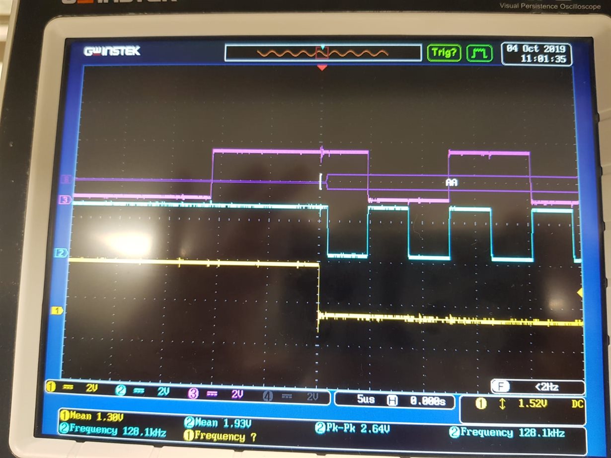
    Initially my DATA was idle low from FPGA and CLK was also idle low. As can be seen from the oscilloscope image below:


    I changed my CLK idle to high and DATA was still kept low. In this scenario, the first DATA bit change should have happened at the rising edge and I should have captured it at the falling edge. But due to DATA idle low, first DATA bit change was happening at the falling edge and my SPI failed to capture that. You can see the image below:


    I managed to fix it by freely floating the DATA pin from the communication transceiver instead of enabling it when I match the SOF. SOF now only activates my CLK output from FPGA whereas DATA output is always enabled. As can be seen from the image below:


    Also DATA freely floating can be understood from the image below:


    But I still fail to understand, why my SPI ISR is not hit when i comment P3SEL |= 0x01, when I am using SPI in 3 pin slave mode.

    STE should not have any role to play with SPI ISR when SPI is used in 3 pin slave mode. Below is the TI code that I am using in my SPI initialization attached in my previous message.


    bool USCI_B_SPI_initSlave(uint16_t baseAddress,
                              uint8_t msbFirst,
                              uint8_t clockPhase,
                              uint8_t clockPolarity)
    {
        //Disable USCI Module
        HWREG8(baseAddress + OFS_UCBxCTL1) |= UCSWRST;
    
        //Reset OFS_UCBxCTL0 register
        HWREG8(baseAddress + OFS_UCBxCTL0) &= ~(UCMSB +
                                                UC7BIT +
                                                UCMST +
                                                UCCKPL +
                                                UCCKPH +
                                                UCMODE_3
                                                );
    
        //Clock polarity, phase select, msbFirst, SYNC, Mode0
        HWREG8(baseAddress + OFS_UCBxCTL0) |= (clockPhase +
                                               clockPolarity +
                                               msbFirst +
                                               UCSYNC +
                                               UCMODE_0
                                               );
    
        return (STATUS_SUCCESS);
    }


    Thanks and Regards,

    Ankit
  • Hi,

    Any issue with my code which is causing the aforementioned problem:

    ..............But I still fail to understand, why my SPI ISR is not hit when i comment P3SEL |= 0x01, when I am using SPI in 3 pin slave mode.

    STE should not have any role to play with SPI ISR when SPI is used in 3 pin slave mode. Below is the TI code that I am using in my SPI initialization attached in my previous message................

  • Ankit,

    You are not using STE.

    Why do you use P3SEL |= 0x01?

  • Hi Dennis,

    Because my SPI slave ISR is never hit if I don't do P3SEL |= 0x01, that doesn't make sense to me either.

    Thanks and Regards,

    Ankit
  • Hi Ankit,

    I'm wondering if this is a bug.

    What is the value of UCBxCTL0 after you initialize the SPI?

    Let me check with the product team to see if they are aware of this.

  • Hi Dennis,

    Sure. I will test it tomorrow and post the results.

    Thanks and Regards,

    Ankit
  • Hi Dennis,

    My UCB0CTL0 value was 0x23. I realised my mistake. In my InitializeUcb0 code I was using USCI_B_SPI_initSlave((uint16_t) USCI_B0_BASE, USCI_B_SPI_MSB_FIRST, 0, 1))

    //Clock polarity, phase select, msbFirst, SYNC, Mode0
    HWREG8(baseAddress + OFS_UCBxCTL0) |= (clockPhase +
    clockPolarity +
    msbFirst +
    UCSYNC +
    UCMODE_0
    );

    For the clock polarity, I was using 1 (0x01)  which should be UCCKPL macro with value 0x40 which was giving the trouble. This was causing the mode to change from 3 pin mode to 4 pin mode.

    After using 0x40, the problem is resolved.

    However, there is something I would like to understand. The problem is only resolved when I change my clock phase also to UCCKPH which is 0x80 which I thought should be 0x00 as per the SPI timing diagram from MSP430F5xx user guide and my signal captured from the oscilloscope:

    According to me it should be Clock Phase as 0x00 and Clock Polarity as UCCKPL. But I lose my first bit in that case and my result becomes 0x55 0x55... and some bits totally wrong.

    However if I use Clock Phase as UCCKPH and Clock Polarity as UCCKPL then my bits are all correct. But I don't understand why it is like that.

    Thanks and Regards,

    Ankit

  • Hi Ankit,

    Yes, I believe UCCKPL should be 1 and UCCKPH should be 0 based on your oscilloscope capture.

    This might be a better diagram.

  • Hi Dennis,

    I read the MSP430F5438A-EP datasheet again.

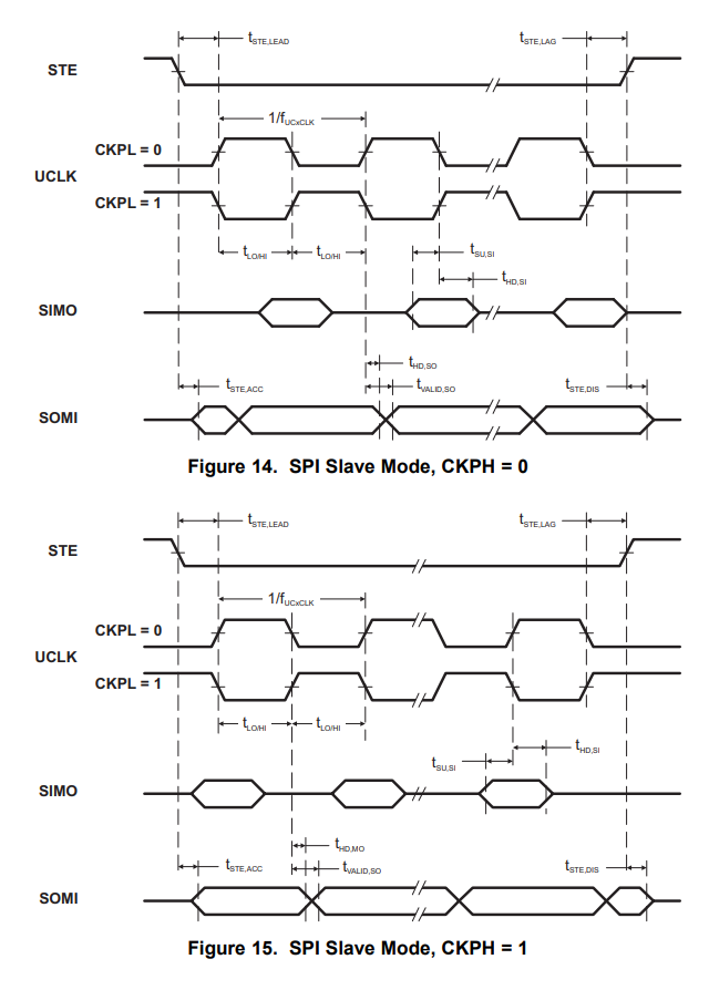
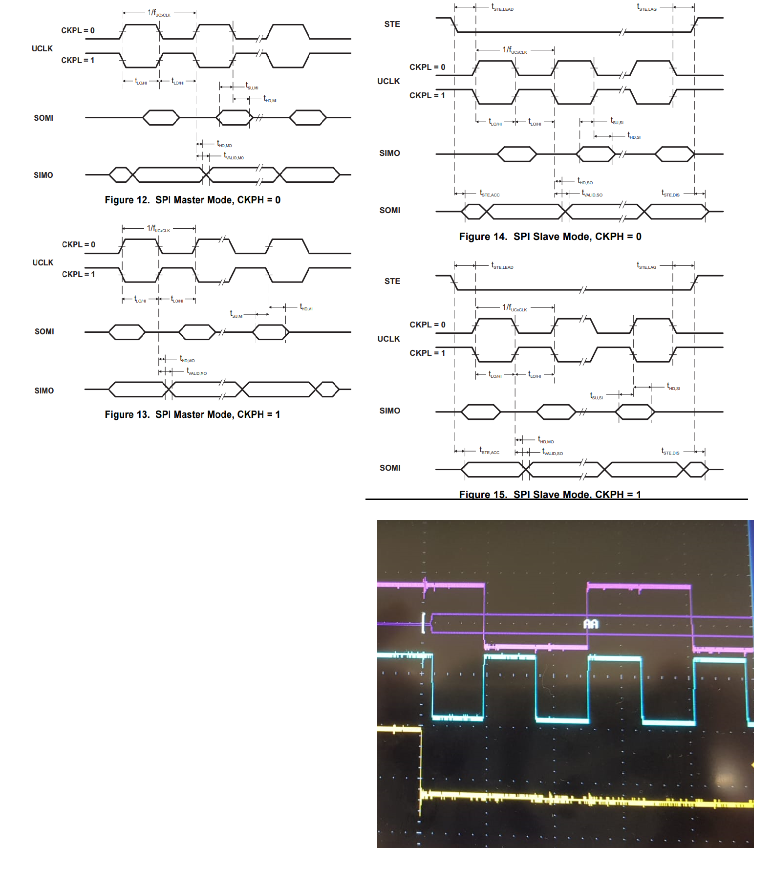
    I realised something. Based on my observation and the figure below (the oscilloscope image and SPI master and slave mode timing diagrams), it seems like clock phase and clock polarity both should be high for MSP430 slave mode.

    In the figure 15 (SPI slave mode with CKPL and CKPH both 1), for SIMO line the figure exactly matches my oscilloscope image (probed at the SPI input to MSP430).

    Is my observation correct?

    Thanks and Regards,

    Ankit

  • Hello Ankit,

    Well, here is how I read it.

    CKPH controls when the data changes or is output by the master.  We can agree that CKPL = 1 is set correctly.

    With CKPL = 1 and CKPH = 1, data is output or changes value on the first 'falling edge' of the CLK. This means on the 'falling edge' both the master and slave will present their data on their respective SIMO/SOMI bus pins.  Data is then latched by the master and slave on the 'rising edge' of the CLK.  Based on your scope capture, that is clearly not the case.

    With CKPL = 1 and CKPH = 0, data is output or changes value on the first 'rising edge' of the CLK.  This means on the 'rising edge' both the master and slave will present their data on their respective SIMO/SOMI bus pins.  Data is then latched by the master and slave on the 'falling edge' of the CLK.  This appears to be in agreement with your scope capture.

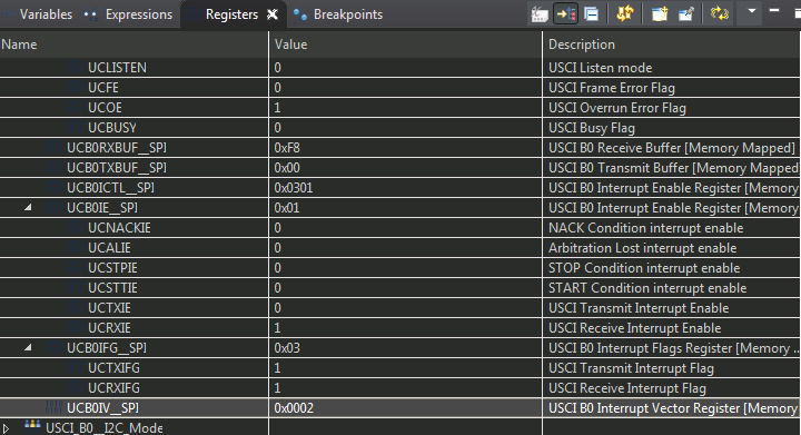
    Let's try this - when you get the SPI communications working, capture all the SPI registers and show me.

  • Hi Dennis,

    Thanks a lot for the explanation.

    In my next reply I will attach the register values.

    Thanks and Regards,

    Ankit

  • Hi Dennis,

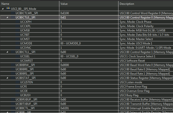
    Please find the SPI Registers screenshot when I initialize the SPI.

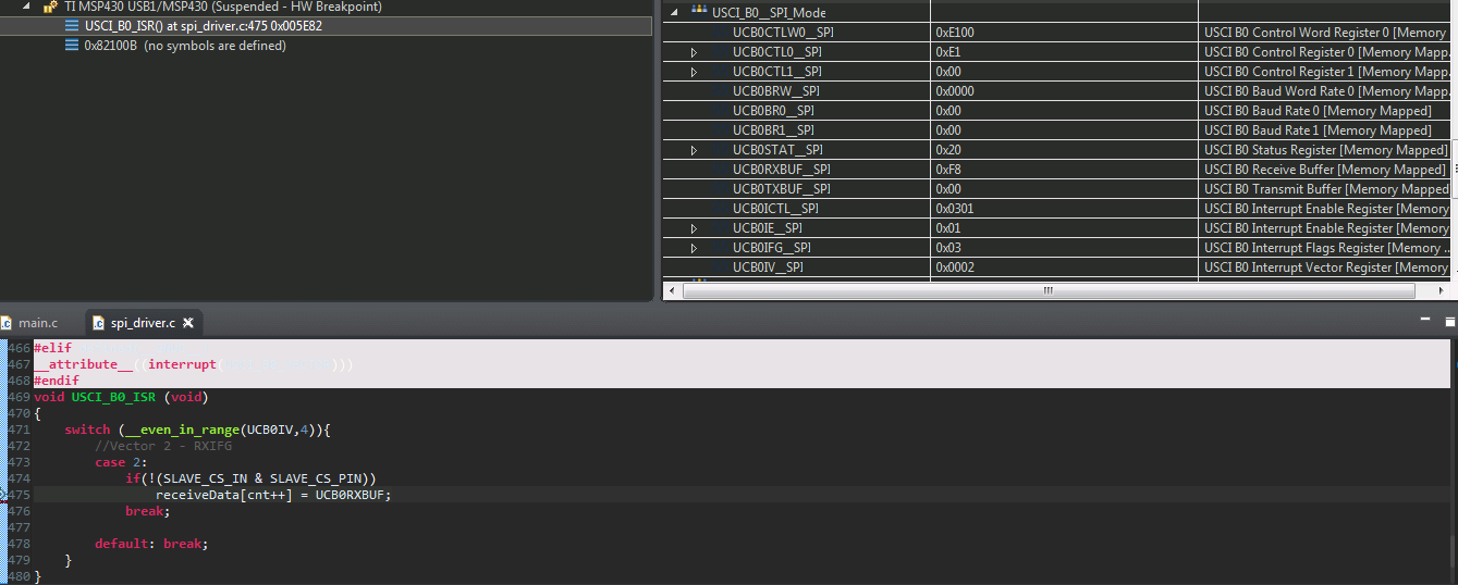
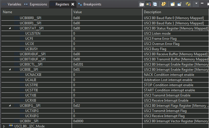
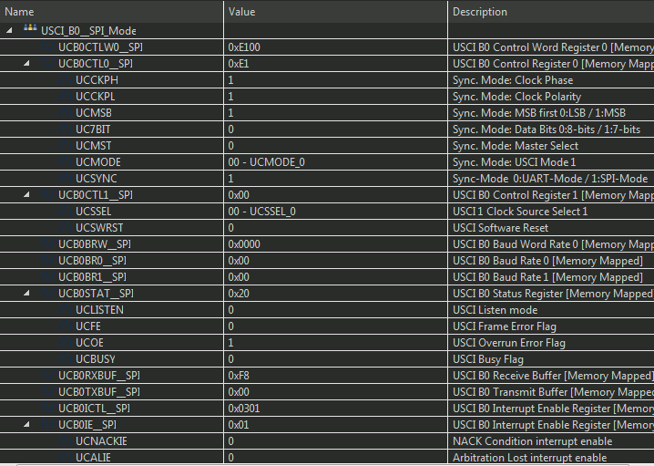
    I have captured the SPI Registers when I receive the first SPI byte as slave from master. Please find the screenshot below:

    Thanks and Regards,

    Ankit

  • Hello Ankit,

    Just make sure whatever CKPL and CKPH settings is used by the master the same are used by the slave.

    If this does not work you then check your master design timing in your FPGA.

**Attention** This is a public forum