This thread has been locked.

If you have a related question, please click the "Ask a related question" button in the top right corner. The newly created question will be automatically linked to this question.

TM4C1294KCPDT: VDDA Shorts VDD

Guru 54077 points
Part Number: TM4C1294KCPDT
Other Parts Discussed in Thread: REF2033

Hello,

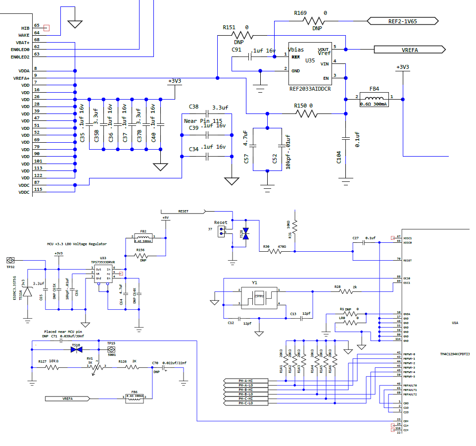
Yet another MCU has early perished powering analog comparator C0+ (PC6) external via REF2033. Note C0+ threshold via RV1 set 2.54v (<3v3) yet VDDA pins 8 to 10 GNDA was (12 ohms), MCU out of circuit. Simply touching DMM probe on TP15 to check C0+ threshold after detecting several unwarranted C0+ faults somehow caused MCU failure. Note wearing static wrist band and PCB outer perimeter foil trace being connect to earth ground, doubtful static was cause.

Besides several TVS diodes did not stop either MCU failure. ADC0/1 are both configured internal VREFA+. Direct powering FB6 from +3v3 does not causes MCU early failure but does allow transients to enter C0+ input, RE2033 seems to provides transient isolation. REF2033 is powered from the same +3v3 LDO as VDD. LR0 being 0R chip or even hard solder bubble to DGND made no difference in post mortem failure analysis.

What is it about configuration also causes VDD to short DGND (<1.3 ohms), MCU out of circuit? Does configuring analog comparators CnO (OR'd outputs OD) have some issue with C0+ external power source? That other configuration VR1 (C0+) powered direct +3v3 worked for several months without failure. Can we damage claim these MCU failures?

  • Devices damaged by electrical overstress (EOS) are typically excluded from claims. Particularly if it occurs during product development.
  • Hi Bob,

    More necessary is to know how can MCU be stressed from 2.54v being placed on PC6 input via REF2033 versus 3v3 LDO? The alternative use of LDO 3v3 on PC6 via RV1 circuit does not lead to VDDA being stressed.

    Otherwise if TM4C1294 requires multilayer PCB to overcome VDD/VDDA rail diode transient it should be specified in design guide two layer PCB may cause MCU rail diode failures. How would TI know if MCU was never tested on dual sided PCB or policy omits customers to send defective devices in for electron microscope analysis?
  • BTW: Notice schematic TPS73533 isolates buck regulator (+5v) AGND from DGND via 20mOhm ferrite bead (not shown) versus copper trace. Notice the REF2033 connects pin 2 to AGND differs from TPS73533 DGND pin 3. Effectively DGND is just above AGND by 75uV 1.84mV ferrite drop @92mA MCU load.

  • We need to know REF2033 with TM4C1294 can GNDA pin 10 short to DGND or mandates same ground as REF2033 uses on pin 2? The datasheet does not make a direct distinction other than statement powering VDDA 1st over VDD when separate supplies are powering ADC module. Yet data sheet states nothing about the analog comparator external VREF source to PC6 being powered from a separate supply. This issue is know as grey area!

  • The requirement that the analog comparator input be between GNDA and VDDA means that the external reference should not be powered on before VDDA.

  • Hi Bob,

    Thanks for your input on this dire issue.

    Bob Crosby said:
    The requirement that the analog comparator input be between GNDA and VDDA means that the external reference should not be powered on before VDDA.

    In retrospect there is certain amount of propagation delay (in/out) REF2033 qualifies for datasheet unclear power cycle timing requirement. Notice MCU shares +3v3 power source R150 powers  VREFA+ (pin 9) as well REF2033 inputs to PC6. The VDD/VDDA shorts occurred MCU powered for several hours after REF2033 was re-configured for PC6 input. Perhaps VREFA+ does not like being powered (R150) when ever PC6 uses same power source and some how VREFA+ (pin9) injection current flows from analog comparator VREF rail into VDD rail?

    Oddly REF2033 never seems to cause an immediate threat to C0+ (PC6) input. There after shorts occur never indication PC6 or any other GPIO used input was damaged or stressed. 

    Can TI please confirm as to how if at all powering external reference (PC6) via REF2033 on even an EVM can lead to VDD/VDDA shorting? Again VDDA to GNDA after short is 12 ohms. Yet VDD/GND 1.3 ohms seems to indicate something else caused VDD short, not REF2033 input to PC6. Could easily be making an incorrect conclusion REF2033 to blame for shorting VDD/VDDA. Again VREFA+ is powered via R150 same as EVM. Though each used internal reference for ADC0/1, the EVM did not have REF2033 connected to analog comparator PC6. Again VDD/VDDA shorts are not occurring during MCU power up, rather occur hours later should c0-,c1-,c2- encounter DC pulse <VDDA MAX (4v). Could VREFA+ (pin 9) somehow cause injection current into VDD rail during such a scenario?

  • REF2033 Turn on delay from datasheet:

    ton   Turn-on time             0.1% settling,  CL = 1 μF          500 μs TYP

    Only recently (coincidently) repopulated C52,C57,R150 to provide power to VREFA+.  Previously solder shorted VREFA+ pin 9 to VDD pin 8, omitting C52,C57,R150 as TPS73533 via FB6 powered c0+ via PC6 being set <2.54vdc. Oddly PC6 is not damaged in the process however  VREFA+ has been effected similar to VDDA 12 ohms.

    Perhaps datasheet omitted critical information, though reference is configured internal, VREFP does not fully disconnect VREFA+ from analog comparator? Scenario, injection current flows VREFA+ (3v3) internally into C0+ PC6 (2.54v) of external threshold reference. Scenario exceeds 440uA (IVREF) at some point when cO0,C01,C02 configured OD are triggered! Note C57 (4.7uf)  is well above 1uf nominal.

    ILVREF: DC leakage current on VREF+ input when external VREF disabled    2.0 μA