This thread has been locked.

If you have a related question, please click the "Ask a related question" button in the top right corner. The newly created question will be automatically linked to this question.

Reading pixel from Kentec 7.0 800x480 SSD1963 on Tiva C Series LaunchPad

Other Parts Discussed in Thread: EK-TM4C123GXL, ENERGIA, ADS7843

I'm using the Kentec 7.0" 800x480 K70DWN2-V1-FF display connected to the EK-TM4C123GXL Tiva C Series LaunchPad —formerly EK-LM4F120XL LaunchPad— through the EB-LM4F120-L35 BoosterPack.

I'm working on the libraries supplied in this package http://www.kentecdisplay.com/Downloads/ek-tm4c123gxl-boost-l35_131216.rar. The Kentec 7.0" 800x480 K70DWN2-V1-FF display uses the SSD1963 controller.

Surprisingly, the read pixel function isn't implemented for the SSD1963.

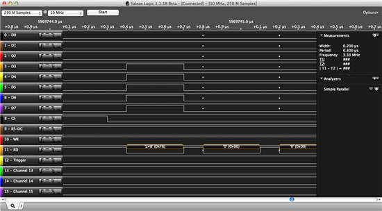
I followed the instruction from the SSD1963 specification sheet but, although the screen sends the correct values 0xf8 0x00 0x00 = red and despite my logic analyser traces them, the port B doesn't read them.

The read pixel works fine for the Kentec 3.5" 320x240 EB-LM4F120-L35 screen, based on the SSD2119.

The major difference between both controllers is: the SSD1963 requires GPIO_STRENGTH_8MA instead of GPIO_STRENGTH_2MA for the SSD2119.

To read from the SSD2119, I'm using

GPIODirModeSet(LCD_DATAH_BASE, LCD_DATAH_PINS, GPIO_DIR_MODE_IN);

Should I add extra parameters to read from the SSD1963

GPIOPadConfigSet(LCD_DATAH_BASE, LCD_DATAH_PINS, GPIO_STRENGTH_8MA, GPIO_PIN_TYPE_STD);

What options should I change?

  • Should GPIO_STRENGTH_8MA be changed for a different value?
  • Should GPIO_PIN_TYPE_STD be changed for GPIO_PIN_TYPE_STD_WPU?
Thank you for your help.
  • Hi Rei,

    What pins are the LCD signals connected to?  You mention port B, the scope traces are named port D and the code refers to port H.  Can you post your actual configuration code for the pins that the LCD signals are connected to?

    Regards,

    Sue

  • Bonsoir Sue,

    Sure!

    Pins configuration...

    //
    // LCD control line GPIO definitions.
    //
    #define LCD_DATAH_PERIPH        SYSCTL_PERIPH_GPIOB
    #define LCD_DATAH_BASE          GPIO_PORTB_BASE
    #define LCD_DATAH_PINS          0xff
    
    #define LCD_CS_PERIPH           SYSCTL_PERIPH_GPIOA
    #define LCD_CS_BASE             GPIO_PORTA_BASE
    #define LCD_CS_PIN              GPIO_PIN_7
    #define LCD_DC_PERIPH           SYSCTL_PERIPH_GPIOA
    #define LCD_DC_BASE             GPIO_PORTA_BASE
    #define LCD_DC_PIN              GPIO_PIN_6
    #define LCD_WR_PERIPH           SYSCTL_PERIPH_GPIOA
    #define LCD_WR_BASE             GPIO_PORTA_BASE
    #define LCD_WR_PIN              GPIO_PIN_5
    #define LCD_RD_PERIPH           SYSCTL_PERIPH_GPIOA
    #define LCD_RD_BASE             GPIO_PORTA_BASE
    #define LCD_RD_PIN              GPIO_PIN_4
    

    ...and...

    	//
        // Enable GPIOs
        //
    	SysCtlPeripheralEnable(SYSCTL_PERIPH_GPIOB);
        SysCtlPeripheralEnable(LCD_DC_PERIPH);
        SysCtlPeripheralEnable(LCD_RD_PERIPH);
        SysCtlPeripheralEnable(LCD_WR_PERIPH);
        SysCtlPeripheralEnable(LCD_CS_PERIPH);
        
        //
        // GPIOs as OUTPUT
        //
        GPIOPinTypeGPIOOutput(GPIO_PORTB_BASE, 0xff);
        GPIOPinTypeGPIOOutput(LCD_DC_BASE, LCD_DC_PIN);
        GPIOPinTypeGPIOOutput(LCD_RD_BASE, LCD_RD_PIN);
        GPIOPinTypeGPIOOutput(LCD_WR_BASE, LCD_WR_PIN);
        GPIOPinTypeGPIOOutput(LCD_CS_BASE, LCD_CS_PIN);
    
        GPIOPadConfigSet(LCD_DATAH_BASE, LCD_DATAH_PINS, GPIO_STRENGTH_8MA, GPIO_PIN_TYPE_STD);
        GPIOPadConfigSet(LCD_DC_BASE, LCD_DC_PIN, GPIO_STRENGTH_8MA, GPIO_PIN_TYPE_STD);
        GPIOPadConfigSet(LCD_RD_BASE, LCD_RD_PIN, GPIO_STRENGTH_8MA, GPIO_PIN_TYPE_STD);
        GPIOPadConfigSet(LCD_WR_BASE, LCD_WR_PIN, GPIO_STRENGTH_8MA, GPIO_PIN_TYPE_STD);
        GPIOPadConfigSet(LCD_CS_BASE, LCD_CS_PIN, GPIO_STRENGTH_8MA, GPIO_PIN_TYPE_STD);
        
        //
        // Set the LCD control pins to their default values.
        //
        GPIOPinWrite(LCD_CS_BASE, LCD_CS_PIN, LCD_CS_PIN);
        GPIOPinWrite(LCD_DATAH_BASE, LCD_DATAH_PINS, 0x00);
        GPIOPinWrite(LCD_DC_BASE, LCD_DC_PIN, 0x00);
        GPIOPinWrite(LCD_RD_BASE, LCD_RD_PIN, LCD_RD_PIN);
        GPIOPinWrite(LCD_WR_BASE, LCD_WR_PIN, LCD_WR_PIN);
        GPIOPinWrite(LCD_CS_BASE, LCD_CS_PIN, 0);
    

    Read sub-function...

    inline uint8_t GET_LCD_DATA()
    {
        return HWREG(LCD_DATAH_BASE + GPIO_O_DATA + (LCD_DATAH_PINS << 2));
    }
    

    ...and function

    uint16_t Screen_K70::_readData16()
    {
        uint16_t data16 = 0;
        uint8_t red, blue, green;
        
    	// Switch to INPUT mode
    //    GPIOPinTypeGPIOInput(GPIO_PORTB_BASE, 0xff);
    
        GPIODirModeSet(LCD_DATAH_BASE, LCD_DATAH_PINS, GPIO_DIR_MODE_IN);
    //    GPIOPadConfigSet(LCD_DATAH_BASE, LCD_DATAH_PINS, GPIO_STRENGTH_8MA, GPIO_PIN_TYPE_STD_WPD);
    //    delay(5);
        
        HWREG(LCD_WR_BASE + GPIO_O_DATA + (LCD_WR_PIN << 2)) = LCD_WR_PIN;
    	HWREG(LCD_CS_BASE + GPIO_O_DATA + (LCD_CS_PIN << 2)) = 0;                   // CS LOW
        
        //
        // Assert the read enable signal.  Do this three times to ensure that we
        // meet the display timing requirements (20nS per instruction at 50MHz
        // means we need to ensure at least 3 instructions between edges on WR)
        //
        // Assert the read enable signal. x10 = 200 ns
        //
        HWREG(LCD_RD_BASE + GPIO_O_DATA + (LCD_RD_PIN << 2)) = 0;
        HWREG(LCD_RD_BASE + GPIO_O_DATA + (LCD_RD_PIN << 2)) = 0;
        HWREG(LCD_RD_BASE + GPIO_O_DATA + (LCD_RD_PIN << 2)) = 0;
        HWREG(LCD_RD_BASE + GPIO_O_DATA + (LCD_RD_PIN << 2)) = 0;
        HWREG(LCD_RD_BASE + GPIO_O_DATA + (LCD_RD_PIN << 2)) = 0;
        HWREG(LCD_RD_BASE + GPIO_O_DATA + (LCD_RD_PIN << 2)) = 0;
        HWREG(LCD_RD_BASE + GPIO_O_DATA + (LCD_RD_PIN << 2)) = 0;
        HWREG(LCD_RD_BASE + GPIO_O_DATA + (LCD_RD_PIN << 2)) = 0;
    
        //
        // Read the dummy first sbyte of the data from the bus.
        //
        uint8_t ui = GET_LCD_DATA();
    //    if (ui > 0) {
            Serial.print("1:");
            Serial.println(ui, HEX);
    //    }
        //
        // Deassert the write enable signal. x5 = 100 ns
        //
        HWREG(LCD_RD_BASE + GPIO_O_DATA + (LCD_RD_PIN << 2)) = LCD_RD_PIN;
        HWREG(LCD_RD_BASE + GPIO_O_DATA + (LCD_RD_PIN << 2)) = LCD_RD_PIN;
        HWREG(LCD_RD_BASE + GPIO_O_DATA + (LCD_RD_PIN << 2)) = LCD_RD_PIN;
        HWREG(LCD_RD_BASE + GPIO_O_DATA + (LCD_RD_PIN << 2)) = LCD_RD_PIN;
        HWREG(LCD_RD_BASE + GPIO_O_DATA + (LCD_RD_PIN << 2)) = LCD_RD_PIN;
        HWREG(LCD_RD_BASE + GPIO_O_DATA + (LCD_RD_PIN << 2)) = LCD_RD_PIN;
        HWREG(LCD_RD_BASE + GPIO_O_DATA + (LCD_RD_PIN << 2)) = LCD_RD_PIN;
        HWREG(LCD_RD_BASE + GPIO_O_DATA + (LCD_RD_PIN << 2)) = LCD_RD_PIN;
        
        //
        // Assert the read enable signal. x10 = 200 ns
        //
        HWREG(LCD_RD_BASE + GPIO_O_DATA + (LCD_RD_PIN << 2)) = 0;
        HWREG(LCD_RD_BASE + GPIO_O_DATA + (LCD_RD_PIN << 2)) = 0;
        HWREG(LCD_RD_BASE + GPIO_O_DATA + (LCD_RD_PIN << 2)) = 0;
        HWREG(LCD_RD_BASE + GPIO_O_DATA + (LCD_RD_PIN << 2)) = 0;
        
        //
        // Read the dummy first sbyte of the data from the bus.
        //
        ui = GET_LCD_DATA();
    //    if (ui > 0) {
            Serial.print("2:");
            Serial.println(ui, HEX);
    //    }
        //
        // Deassert the write enable signal. x5 = 100 ns
        //
        HWREG(LCD_RD_BASE + GPIO_O_DATA + (LCD_RD_PIN << 2)) = LCD_RD_PIN;
        HWREG(LCD_RD_BASE + GPIO_O_DATA + (LCD_RD_PIN << 2)) = LCD_RD_PIN;
        HWREG(LCD_RD_BASE + GPIO_O_DATA + (LCD_RD_PIN << 2)) = LCD_RD_PIN;
        HWREG(LCD_RD_BASE + GPIO_O_DATA + (LCD_RD_PIN << 2)) = LCD_RD_PIN;
        HWREG(LCD_RD_BASE + GPIO_O_DATA + (LCD_RD_PIN << 2)) = LCD_RD_PIN;
        HWREG(LCD_RD_BASE + GPIO_O_DATA + (LCD_RD_PIN << 2)) = LCD_RD_PIN;
        HWREG(LCD_RD_BASE + GPIO_O_DATA + (LCD_RD_PIN << 2)) = LCD_RD_PIN;
        HWREG(LCD_RD_BASE + GPIO_O_DATA + (LCD_RD_PIN << 2)) = LCD_RD_PIN;
        
        //
        // Assert the read enable signal. x10 = 200 ns
        //
        HWREG(LCD_RD_BASE + GPIO_O_DATA + (LCD_RD_PIN << 2)) = 0;
        HWREG(LCD_RD_BASE + GPIO_O_DATA + (LCD_RD_PIN << 2)) = 0;
        HWREG(LCD_RD_BASE + GPIO_O_DATA + (LCD_RD_PIN << 2)) = 0;
        HWREG(LCD_RD_BASE + GPIO_O_DATA + (LCD_RD_PIN << 2)) = 0;
        
        //
        // Read the most significant byte of the data from the bus.
        //
        //    data16   = (GET_LCD_DATA() >>3) <<11;
        red = GET_LCD_DATA();
    //    if (ui > 0) {
            Serial.print("3:");
            Serial.println(red, HEX);
    //    }
        //
        // Deassert the read enable signal. x5 = 100 ns
        //
        HWREG(LCD_RD_BASE + GPIO_O_DATA + (LCD_RD_PIN << 2)) = LCD_RD_PIN;
        HWREG(LCD_RD_BASE + GPIO_O_DATA + (LCD_RD_PIN << 2)) = LCD_RD_PIN;
        HWREG(LCD_RD_BASE + GPIO_O_DATA + (LCD_RD_PIN << 2)) = LCD_RD_PIN;
        HWREG(LCD_RD_BASE + GPIO_O_DATA + (LCD_RD_PIN << 2)) = LCD_RD_PIN;
        HWREG(LCD_RD_BASE + GPIO_O_DATA + (LCD_RD_PIN << 2)) = LCD_RD_PIN;
        HWREG(LCD_RD_BASE + GPIO_O_DATA + (LCD_RD_PIN << 2)) = LCD_RD_PIN;
        HWREG(LCD_RD_BASE + GPIO_O_DATA + (LCD_RD_PIN << 2)) = LCD_RD_PIN;
        HWREG(LCD_RD_BASE + GPIO_O_DATA + (LCD_RD_PIN << 2)) = LCD_RD_PIN;
        
        //
        // Assert the read enable signal. x10 = 200 ns
        //
        HWREG(LCD_RD_BASE + GPIO_O_DATA + (LCD_RD_PIN << 2)) = 0;
        HWREG(LCD_RD_BASE + GPIO_O_DATA + (LCD_RD_PIN << 2)) = 0;
        HWREG(LCD_RD_BASE + GPIO_O_DATA + (LCD_RD_PIN << 2)) = 0;
        HWREG(LCD_RD_BASE + GPIO_O_DATA + (LCD_RD_PIN << 2)) = 0;
        
        //
        // Read the least significant byte of the data from the bus.
        //
        //    data16   |= (GET_LCD_DATA() >> 2) << 5;
        green = GET_LCD_DATA();
    //    if (ui > 0) {
            Serial.print("4:");
            Serial.println(green, HEX);
    //    }
        //
        // Deassert the read enable signal. x5 = 100 ns
        //
        HWREG(LCD_RD_BASE + GPIO_O_DATA + (LCD_RD_PIN << 2)) = LCD_RD_PIN;
        HWREG(LCD_RD_BASE + GPIO_O_DATA + (LCD_RD_PIN << 2)) = LCD_RD_PIN;
        HWREG(LCD_RD_BASE + GPIO_O_DATA + (LCD_RD_PIN << 2)) = LCD_RD_PIN;
        HWREG(LCD_RD_BASE + GPIO_O_DATA + (LCD_RD_PIN << 2)) = LCD_RD_PIN;
        HWREG(LCD_RD_BASE + GPIO_O_DATA + (LCD_RD_PIN << 2)) = LCD_RD_PIN;
        HWREG(LCD_RD_BASE + GPIO_O_DATA + (LCD_RD_PIN << 2)) = LCD_RD_PIN;
        HWREG(LCD_RD_BASE + GPIO_O_DATA + (LCD_RD_PIN << 2)) = LCD_RD_PIN;
        HWREG(LCD_RD_BASE + GPIO_O_DATA + (LCD_RD_PIN << 2)) = LCD_RD_PIN;
        
        //
        // Assert the read enable signal. x10 = 200 ns
        //
        HWREG(LCD_RD_BASE + GPIO_O_DATA + (LCD_RD_PIN << 2)) = 0;
        HWREG(LCD_RD_BASE + GPIO_O_DATA + (LCD_RD_PIN << 2)) = 0;
        HWREG(LCD_RD_BASE + GPIO_O_DATA + (LCD_RD_PIN << 2)) = 0;
        HWREG(LCD_RD_BASE + GPIO_O_DATA + (LCD_RD_PIN << 2)) = 0;
        
        //
        // Read the least significant byte of the data from the bus.
        //
        //    data16   |= (GET_LCD_DATA() >>3);
        blue = GET_LCD_DATA();
    //    if (ui > 0) {
            Serial.print("5:");
            Serial.println(blue, HEX);
    //    }
        //
        // Deassert the read enable signal.
        //
        HWREG(LCD_RD_BASE + GPIO_O_DATA + (LCD_RD_PIN << 2)) = LCD_RD_PIN;
        HWREG(LCD_RD_BASE + GPIO_O_DATA + (LCD_RD_PIN << 2)) = LCD_RD_PIN;
        HWREG(LCD_RD_BASE + GPIO_O_DATA + (LCD_RD_PIN << 2)) = LCD_RD_PIN;
        HWREG(LCD_RD_BASE + GPIO_O_DATA + (LCD_RD_PIN << 2)) = LCD_RD_PIN;
        HWREG(LCD_RD_BASE + GPIO_O_DATA + (LCD_RD_PIN << 2)) = LCD_RD_PIN;
        HWREG(LCD_RD_BASE + GPIO_O_DATA + (LCD_RD_PIN << 2)) = LCD_RD_PIN;
        HWREG(LCD_RD_BASE + GPIO_O_DATA + (LCD_RD_PIN << 2)) = LCD_RD_PIN;
        HWREG(LCD_RD_BASE + GPIO_O_DATA + (LCD_RD_PIN << 2)) = LCD_RD_PIN;
        //    HWREG(LCD_WR_BASE + GPIO_O_DATA + (LCD_RD_PIN << 2)) = LCD_RD_PIN;
        
        HWREG(LCD_CS_BASE + GPIO_O_DATA + (LCD_CS_PIN << 2)) = LCD_CS_PIN;          // CS HIGH
        
        // Return to OUTPUT mode
    //    GPIOPinTypeGPIOOutput(GPIO_PORTB_BASE, 0xff);
        GPIODirModeSet(LCD_DATAH_BASE, LCD_DATAH_PINS, GPIO_DIR_MODE_OUT);
        GPIOPadConfigSet(LCD_DATAH_BASE, LCD_DATAH_PINS, GPIO_STRENGTH_8MA, GPIO_PIN_TYPE_STD);
        
        data16 = (red >>3) <<11 | (green >>2) <<5 | blue >>3;
        return data16;
    }
    

    The D-ports on the logic analysers are connected to the LCD_DATAH_PERIPH = SYSCTL_PERIPH_GPIOB port.

    Output is

    Kentec 7" screen

    800x480

    1:0

    2:0

    3:0

    4:0

    5:0

    0

    ---

  • Hi Rei,

    Thanks for the additional information.  When you say that the Tiva MCU does not get the value of 0xf8, What does the MCU read?

    It appears from the logic analyzer tracing that the read signal goes high at the same time the data goes away.  I'm not familiar with the timings on the Kentec display, but is it possible that the read signal should go high before the data goes away?  Maybe:

        //
        // Assert the read enable signal. x10 = 200 ns
        //
        HWREG(LCD_RD_BASE + GPIO_O_DATA + (LCD_RD_PIN << 2)) = 0;
        HWREG(LCD_RD_BASE + GPIO_O_DATA + (LCD_RD_PIN << 2)) = 0;
        HWREG(LCD_RD_BASE + GPIO_O_DATA + (LCD_RD_PIN << 2)) = 0;
        HWREG(LCD_RD_BASE + GPIO_O_DATA + (LCD_RD_PIN << 2)) = 0;
        
        //
        // Read the least significant byte of the data from the bus.
        //
        //    data16   |= (GET_LCD_DATA() >> 2) << 5;
        green = GET_LCD_DATA();
    //    if (ui > 0) {
            Serial.print("4:");
            Serial.println(green, HEX);
    //    }
        HWREG(LCD_RD_BASE + GPIO_O_DATA + (LCD_RD_PIN << 2)) = 0;
        HWREG(LCD_RD_BASE + GPIO_O_DATA + (LCD_RD_PIN << 2)) = 0;
        //
        // Deassert the read enable signal. x5 = 100 ns
        //
        HWREG(LCD_RD_BASE + GPIO_O_DATA + (LCD_RD_PIN << 2)) = LCD_RD_PIN;
        HWREG(LCD_RD_BASE + GPIO_O_DATA + (LCD_RD_PIN << 2)) = LCD_RD_PIN;
        HWREG(LCD_RD_BASE + GPIO_O_DATA + (LCD_RD_PIN << 2)) = LCD_RD_PIN;
        HWREG(LCD_RD_BASE + GPIO_O_DATA + (LCD_RD_PIN << 2)) = LCD_RD_PIN;
        HWREG(LCD_RD_BASE + GPIO_O_DATA + (LCD_RD_PIN << 2)) = LCD_RD_PIN;
        HWREG(LCD_RD_BASE + GPIO_O_DATA + (LCD_RD_PIN << 2)) = LCD_RD_PIN;
        HWREG(LCD_RD_BASE + GPIO_O_DATA + (LCD_RD_PIN << 2)) = LCD_RD_PIN;
        HWREG(LCD_RD_BASE + GPIO_O_DATA + (LCD_RD_PIN << 2)) = LCD_RD_PIN;
  • Thank you for your message. I tried the new approach, reading the value twice. Unfortunately, result is still 0.

    Kentec 7" screen
    800x480
    1:0
    1*:0
    2:0
    2*:0
    3:0
    3*:0
    4:0
    4*:0
    5:0
    5*:0
    0
    ---

    Is the GPIO port correctly configured?

    The SSD1963 requires GPIO_STRENGTH_8MA with the port is in output mode, so is there a specific parameter when the port is in input mode?

    uint16_t Screen_K70::_readData16()
    {
        uint16_t data16 = 0;
        uint8_t red, blue, green;
        
    	// Switch to INPUT mode
        //    GPIOPinTypeGPIOInput(GPIO_PORTB_BASE, 0xff);
        //    SET_LCD_DATA(0xff);
        
        GPIODirModeSet(LCD_DATAH_BASE, LCD_DATAH_PINS, GPIO_DIR_MODE_IN);
        //    GPIOPadConfigSet(LCD_DATAH_BASE, LCD_DATAH_PINS, GPIO_STRENGTH_2MA, GPIO_PIN_TYPE_STD_WPD);
        //    delay(5);
        //    GPIOPadConfigSet(LCD_DATAH_BASE, LCD_DATAH_PINS, GPIO_STRENGTH_2MA, GPIO_PIN_TYPE_OD);
        
        //
        // Deassert the read enable signal.
        // Deassert the write enable signal.
        //
        HWREG(LCD_RD_BASE + GPIO_O_DATA + (LCD_RD_PIN << 2)) = LCD_RD_PIN;
        HWREG(LCD_WR_BASE + GPIO_O_DATA + (LCD_RD_PIN << 2)) = LCD_WR_PIN;
        
    	HWREG(LCD_CS_BASE + GPIO_O_DATA + (LCD_CS_PIN << 2)) = 0;                   // CS LOW
        
        //
        // Assert the read enable signal.  Do this three times to ensure that we
        // meet the display timing requirements (20nS per instruction at 50MHz
        // means we need to ensure at least 3 instructions between edges on WR)
        //
        // Assert the read enable signal. x10 = 200 ns
        //
        HWREG(LCD_RD_BASE + GPIO_O_DATA + (LCD_RD_PIN << 2)) = 0;
        HWREG(LCD_RD_BASE + GPIO_O_DATA + (LCD_RD_PIN << 2)) = 0;
        HWREG(LCD_RD_BASE + GPIO_O_DATA + (LCD_RD_PIN << 2)) = 0;
        HWREG(LCD_RD_BASE + GPIO_O_DATA + (LCD_RD_PIN << 2)) = 0;
        HWREG(LCD_RD_BASE + GPIO_O_DATA + (LCD_RD_PIN << 2)) = 0;
        HWREG(LCD_RD_BASE + GPIO_O_DATA + (LCD_RD_PIN << 2)) = 0;
        HWREG(LCD_RD_BASE + GPIO_O_DATA + (LCD_RD_PIN << 2)) = 0;
        HWREG(LCD_RD_BASE + GPIO_O_DATA + (LCD_RD_PIN << 2)) = 0;
        HWREG(LCD_RD_BASE + GPIO_O_DATA + (LCD_RD_PIN << 2)) = 0;
        HWREG(LCD_RD_BASE + GPIO_O_DATA + (LCD_RD_PIN << 2)) = 0;
    
        //
        // Read the dummy first sbyte of the data from the bus.
        //
        uint8_t ui = GET_LCD_DATA();
        Serial.print("1:");
        Serial.println(ui, HEX);
    
        //
        // Deassert the read enable signal. x5 = 100 ns
        //
        HWREG(LCD_RD_BASE + GPIO_O_DATA + (LCD_RD_PIN << 2)) = LCD_RD_PIN;
        HWREG(LCD_RD_BASE + GPIO_O_DATA + (LCD_RD_PIN << 2)) = LCD_RD_PIN;
        HWREG(LCD_RD_BASE + GPIO_O_DATA + (LCD_RD_PIN << 2)) = LCD_RD_PIN;
        HWREG(LCD_RD_BASE + GPIO_O_DATA + (LCD_RD_PIN << 2)) = LCD_RD_PIN;
        HWREG(LCD_RD_BASE + GPIO_O_DATA + (LCD_RD_PIN << 2)) = LCD_RD_PIN;
        HWREG(LCD_RD_BASE + GPIO_O_DATA + (LCD_RD_PIN << 2)) = LCD_RD_PIN;
        HWREG(LCD_RD_BASE + GPIO_O_DATA + (LCD_RD_PIN << 2)) = LCD_RD_PIN;
        HWREG(LCD_RD_BASE + GPIO_O_DATA + (LCD_RD_PIN << 2)) = LCD_RD_PIN;
        HWREG(LCD_RD_BASE + GPIO_O_DATA + (LCD_RD_PIN << 2)) = LCD_RD_PIN;
        HWREG(LCD_RD_BASE + GPIO_O_DATA + (LCD_RD_PIN << 2)) = LCD_RD_PIN;
        
        ui = GET_LCD_DATA();
        Serial.print("1*:");
        Serial.println(ui, HEX);
    
        //
        // Assert the read enable signal. x10 = 200 ns
        //
        HWREG(LCD_RD_BASE + GPIO_O_DATA + (LCD_RD_PIN << 2)) = 0;
        HWREG(LCD_RD_BASE + GPIO_O_DATA + (LCD_RD_PIN << 2)) = 0;
        HWREG(LCD_RD_BASE + GPIO_O_DATA + (LCD_RD_PIN << 2)) = 0;
        HWREG(LCD_RD_BASE + GPIO_O_DATA + (LCD_RD_PIN << 2)) = 0;
        HWREG(LCD_RD_BASE + GPIO_O_DATA + (LCD_RD_PIN << 2)) = 0;
        HWREG(LCD_RD_BASE + GPIO_O_DATA + (LCD_RD_PIN << 2)) = 0;
        HWREG(LCD_RD_BASE + GPIO_O_DATA + (LCD_RD_PIN << 2)) = 0;
        HWREG(LCD_RD_BASE + GPIO_O_DATA + (LCD_RD_PIN << 2)) = 0;
        HWREG(LCD_RD_BASE + GPIO_O_DATA + (LCD_RD_PIN << 2)) = 0;
        HWREG(LCD_RD_BASE + GPIO_O_DATA + (LCD_RD_PIN << 2)) = 0;
        
        //
        // Read the dummy first sbyte of the data from the bus.
        //
        ui = GET_LCD_DATA();
        Serial.print("2:");
        Serial.println(ui, HEX);
    
        //
        // Deassert the read enable signal. x5 = 100 ns
        //
        HWREG(LCD_RD_BASE + GPIO_O_DATA + (LCD_RD_PIN << 2)) = LCD_RD_PIN;
        HWREG(LCD_RD_BASE + GPIO_O_DATA + (LCD_RD_PIN << 2)) = LCD_RD_PIN;
        HWREG(LCD_RD_BASE + GPIO_O_DATA + (LCD_RD_PIN << 2)) = LCD_RD_PIN;
        HWREG(LCD_RD_BASE + GPIO_O_DATA + (LCD_RD_PIN << 2)) = LCD_RD_PIN;
        HWREG(LCD_RD_BASE + GPIO_O_DATA + (LCD_RD_PIN << 2)) = LCD_RD_PIN;
        HWREG(LCD_RD_BASE + GPIO_O_DATA + (LCD_RD_PIN << 2)) = LCD_RD_PIN;
        HWREG(LCD_RD_BASE + GPIO_O_DATA + (LCD_RD_PIN << 2)) = LCD_RD_PIN;
        HWREG(LCD_RD_BASE + GPIO_O_DATA + (LCD_RD_PIN << 2)) = LCD_RD_PIN;
        HWREG(LCD_RD_BASE + GPIO_O_DATA + (LCD_RD_PIN << 2)) = LCD_RD_PIN;
        HWREG(LCD_RD_BASE + GPIO_O_DATA + (LCD_RD_PIN << 2)) = LCD_RD_PIN;
    
        ui = GET_LCD_DATA();
        Serial.print("2*:");
        Serial.println(ui, HEX);
    
        //
        // Assert the read enable signal. x10 = 200 ns
        //
        HWREG(LCD_RD_BASE + GPIO_O_DATA + (LCD_RD_PIN << 2)) = 0;
        HWREG(LCD_RD_BASE + GPIO_O_DATA + (LCD_RD_PIN << 2)) = 0;
        HWREG(LCD_RD_BASE + GPIO_O_DATA + (LCD_RD_PIN << 2)) = 0;
        HWREG(LCD_RD_BASE + GPIO_O_DATA + (LCD_RD_PIN << 2)) = 0;
        HWREG(LCD_RD_BASE + GPIO_O_DATA + (LCD_RD_PIN << 2)) = 0;
        HWREG(LCD_RD_BASE + GPIO_O_DATA + (LCD_RD_PIN << 2)) = 0;
        HWREG(LCD_RD_BASE + GPIO_O_DATA + (LCD_RD_PIN << 2)) = 0;
        HWREG(LCD_RD_BASE + GPIO_O_DATA + (LCD_RD_PIN << 2)) = 0;
        HWREG(LCD_RD_BASE + GPIO_O_DATA + (LCD_RD_PIN << 2)) = 0;
        HWREG(LCD_RD_BASE + GPIO_O_DATA + (LCD_RD_PIN << 2)) = 0;
        
        //
        // Read the most significant byte of the data from the bus.
        //
        //    data16   = (GET_LCD_DATA() >>3) <<11;
        red = GET_LCD_DATA();
        Serial.print("3:");
        Serial.println(red, HEX);
    
        //
        // Deassert the read enable signal. x5 = 100 ns
        //
        HWREG(LCD_RD_BASE + GPIO_O_DATA + (LCD_RD_PIN << 2)) = LCD_RD_PIN;
        HWREG(LCD_RD_BASE + GPIO_O_DATA + (LCD_RD_PIN << 2)) = LCD_RD_PIN;
        HWREG(LCD_RD_BASE + GPIO_O_DATA + (LCD_RD_PIN << 2)) = LCD_RD_PIN;
        HWREG(LCD_RD_BASE + GPIO_O_DATA + (LCD_RD_PIN << 2)) = LCD_RD_PIN;
        HWREG(LCD_RD_BASE + GPIO_O_DATA + (LCD_RD_PIN << 2)) = LCD_RD_PIN;
        HWREG(LCD_RD_BASE + GPIO_O_DATA + (LCD_RD_PIN << 2)) = LCD_RD_PIN;
        HWREG(LCD_RD_BASE + GPIO_O_DATA + (LCD_RD_PIN << 2)) = LCD_RD_PIN;
        HWREG(LCD_RD_BASE + GPIO_O_DATA + (LCD_RD_PIN << 2)) = LCD_RD_PIN;
        HWREG(LCD_RD_BASE + GPIO_O_DATA + (LCD_RD_PIN << 2)) = LCD_RD_PIN;
        HWREG(LCD_RD_BASE + GPIO_O_DATA + (LCD_RD_PIN << 2)) = LCD_RD_PIN;
    
        ui = GET_LCD_DATA();
        Serial.print("3*:");
        Serial.println(red, HEX);
        
        //
        // Assert the read enable signal. x10 = 200 ns
        //
        HWREG(LCD_RD_BASE + GPIO_O_DATA + (LCD_RD_PIN << 2)) = 0;
        HWREG(LCD_RD_BASE + GPIO_O_DATA + (LCD_RD_PIN << 2)) = 0;
        HWREG(LCD_RD_BASE + GPIO_O_DATA + (LCD_RD_PIN << 2)) = 0;
        HWREG(LCD_RD_BASE + GPIO_O_DATA + (LCD_RD_PIN << 2)) = 0;
        HWREG(LCD_RD_BASE + GPIO_O_DATA + (LCD_RD_PIN << 2)) = 0;
        HWREG(LCD_RD_BASE + GPIO_O_DATA + (LCD_RD_PIN << 2)) = 0;
        HWREG(LCD_RD_BASE + GPIO_O_DATA + (LCD_RD_PIN << 2)) = 0;
        HWREG(LCD_RD_BASE + GPIO_O_DATA + (LCD_RD_PIN << 2)) = 0;
        HWREG(LCD_RD_BASE + GPIO_O_DATA + (LCD_RD_PIN << 2)) = 0;
        HWREG(LCD_RD_BASE + GPIO_O_DATA + (LCD_RD_PIN << 2)) = 0;
        
        //
        // Read the least significant byte of the data from the bus.
        //
        //    data16   |= (GET_LCD_DATA() >> 2) << 5;
        green = GET_LCD_DATA();
        Serial.print("4:");
        Serial.println(green, HEX);
    
        //
        // Deassert the read enable signal. x5 = 100 ns
        //
        HWREG(LCD_RD_BASE + GPIO_O_DATA + (LCD_RD_PIN << 2)) = LCD_RD_PIN;
        HWREG(LCD_RD_BASE + GPIO_O_DATA + (LCD_RD_PIN << 2)) = LCD_RD_PIN;
        HWREG(LCD_RD_BASE + GPIO_O_DATA + (LCD_RD_PIN << 2)) = LCD_RD_PIN;
        HWREG(LCD_RD_BASE + GPIO_O_DATA + (LCD_RD_PIN << 2)) = LCD_RD_PIN;
        HWREG(LCD_RD_BASE + GPIO_O_DATA + (LCD_RD_PIN << 2)) = LCD_RD_PIN;
        HWREG(LCD_RD_BASE + GPIO_O_DATA + (LCD_RD_PIN << 2)) = LCD_RD_PIN;
        HWREG(LCD_RD_BASE + GPIO_O_DATA + (LCD_RD_PIN << 2)) = LCD_RD_PIN;
        HWREG(LCD_RD_BASE + GPIO_O_DATA + (LCD_RD_PIN << 2)) = LCD_RD_PIN;
        HWREG(LCD_RD_BASE + GPIO_O_DATA + (LCD_RD_PIN << 2)) = LCD_RD_PIN;
        HWREG(LCD_RD_BASE + GPIO_O_DATA + (LCD_RD_PIN << 2)) = LCD_RD_PIN;
    
        ui = GET_LCD_DATA();
        Serial.print("4*:");
        Serial.println(red, HEX);
        
        //
        // Assert the read enable signal. x10 = 200 ns
        //
        HWREG(LCD_RD_BASE + GPIO_O_DATA + (LCD_RD_PIN << 2)) = 0;
        HWREG(LCD_RD_BASE + GPIO_O_DATA + (LCD_RD_PIN << 2)) = 0;
        HWREG(LCD_RD_BASE + GPIO_O_DATA + (LCD_RD_PIN << 2)) = 0;
        HWREG(LCD_RD_BASE + GPIO_O_DATA + (LCD_RD_PIN << 2)) = 0;
        HWREG(LCD_RD_BASE + GPIO_O_DATA + (LCD_RD_PIN << 2)) = 0;
        HWREG(LCD_RD_BASE + GPIO_O_DATA + (LCD_RD_PIN << 2)) = 0;
        HWREG(LCD_RD_BASE + GPIO_O_DATA + (LCD_RD_PIN << 2)) = 0;
        HWREG(LCD_RD_BASE + GPIO_O_DATA + (LCD_RD_PIN << 2)) = 0;
        HWREG(LCD_RD_BASE + GPIO_O_DATA + (LCD_RD_PIN << 2)) = 0;
        HWREG(LCD_RD_BASE + GPIO_O_DATA + (LCD_RD_PIN << 2)) = 0;
        
        //
        // Read the least significant byte of the data from the bus.
        //
        //    data16   |= (GET_LCD_DATA() >>3);
        blue = GET_LCD_DATA();
        Serial.print("5:");
        Serial.println(blue, HEX);
        
        //
        // Deassert the read enable signal.
        //
        HWREG(LCD_RD_BASE + GPIO_O_DATA + (LCD_RD_PIN << 2)) = LCD_RD_PIN;
        HWREG(LCD_RD_BASE + GPIO_O_DATA + (LCD_RD_PIN << 2)) = LCD_RD_PIN;
        HWREG(LCD_RD_BASE + GPIO_O_DATA + (LCD_RD_PIN << 2)) = LCD_RD_PIN;
        HWREG(LCD_RD_BASE + GPIO_O_DATA + (LCD_RD_PIN << 2)) = LCD_RD_PIN;
        HWREG(LCD_RD_BASE + GPIO_O_DATA + (LCD_RD_PIN << 2)) = LCD_RD_PIN;
        HWREG(LCD_RD_BASE + GPIO_O_DATA + (LCD_RD_PIN << 2)) = LCD_RD_PIN;
        HWREG(LCD_RD_BASE + GPIO_O_DATA + (LCD_RD_PIN << 2)) = LCD_RD_PIN;
        HWREG(LCD_RD_BASE + GPIO_O_DATA + (LCD_RD_PIN << 2)) = LCD_RD_PIN;
        HWREG(LCD_RD_BASE + GPIO_O_DATA + (LCD_RD_PIN << 2)) = LCD_RD_PIN;
        HWREG(LCD_RD_BASE + GPIO_O_DATA + (LCD_RD_PIN << 2)) = LCD_RD_PIN;
        
        ui = GET_LCD_DATA();
        Serial.print("5*:");
        Serial.println(red, HEX);
        
        HWREG(LCD_CS_BASE + GPIO_O_DATA + (LCD_CS_PIN << 2)) = LCD_CS_PIN;          // CS HIGH
        
        // Return to OUTPUT mode
        //    GPIOPinTypeGPIOOutput(GPIO_PORTB_BASE, 0xff);
        GPIODirModeSet(LCD_DATAH_BASE, LCD_DATAH_PINS, GPIO_DIR_MODE_OUT);
        GPIOPadConfigSet(LCD_DATAH_BASE, LCD_DATAH_PINS, GPIO_STRENGTH_8MA, GPIO_PIN_TYPE_STD);
        
        data16 = (red >>3) <<11 | (green >>2) <<5 | blue >>3;
        return data16;
    }
    

  • The port appears to be properly configured.  The drive strength parameter is only relevant when the pin is in output mode.  I wasn't asking you to read the value twice. I was asking you to keep the read signal low after reading the data for some time.  Have you contacted Kentec for help on this issue?  It is their driver, and they may have better insight into what the problem might be.

    Regards,

    Sue

  • I also tested with the RD signal low kept after reading the data. Same result.

    I'm waiting for an answer from Kentec.

    Thank you for your help.

    uint16_t Screen_K70::_readData16()
    {
        uint16_t data16 = 0;
        uint8_t red, blue, green;
        
    	// Switch to INPUT mode
        //    GPIOPinTypeGPIOInput(GPIO_PORTB_BASE, 0xff);
        //    SET_LCD_DATA(0xff);
        
        GPIODirModeSet(LCD_DATAH_BASE, LCD_DATAH_PINS, GPIO_DIR_MODE_IN);
        //    GPIOPadConfigSet(LCD_DATAH_BASE, LCD_DATAH_PINS, GPIO_STRENGTH_2MA, GPIO_PIN_TYPE_STD_WPD);
        //    delay(5);
        //    GPIOPadConfigSet(LCD_DATAH_BASE, LCD_DATAH_PINS, GPIO_STRENGTH_2MA, GPIO_PIN_TYPE_OD);
        
        //
        // Deassert the read enable signal.
        // Deassert the write enable signal.
        //
        HWREG(LCD_RD_BASE + GPIO_O_DATA + (LCD_RD_PIN << 2)) = LCD_RD_PIN;
        HWREG(LCD_WR_BASE + GPIO_O_DATA + (LCD_RD_PIN << 2)) = LCD_WR_PIN;
        
    	HWREG(LCD_CS_BASE + GPIO_O_DATA + (LCD_CS_PIN << 2)) = 0;                   // CS LOW
        
        //
        // Assert the read enable signal.  Do this three times to ensure that we
        // meet the display timing requirements (20nS per instruction at 50MHz
        // means we need to ensure at least 3 instructions between edges on WR)
        //
        // Assert the read enable signal. x10 = 200 ns
        //
        HWREG(LCD_RD_BASE + GPIO_O_DATA + (LCD_RD_PIN << 2)) = 0;
        HWREG(LCD_RD_BASE + GPIO_O_DATA + (LCD_RD_PIN << 2)) = 0;
        HWREG(LCD_RD_BASE + GPIO_O_DATA + (LCD_RD_PIN << 2)) = 0;
        HWREG(LCD_RD_BASE + GPIO_O_DATA + (LCD_RD_PIN << 2)) = 0;
        HWREG(LCD_RD_BASE + GPIO_O_DATA + (LCD_RD_PIN << 2)) = 0;
        HWREG(LCD_RD_BASE + GPIO_O_DATA + (LCD_RD_PIN << 2)) = 0;
        HWREG(LCD_RD_BASE + GPIO_O_DATA + (LCD_RD_PIN << 2)) = 0;
        HWREG(LCD_RD_BASE + GPIO_O_DATA + (LCD_RD_PIN << 2)) = 0;
        HWREG(LCD_RD_BASE + GPIO_O_DATA + (LCD_RD_PIN << 2)) = 0;
        HWREG(LCD_RD_BASE + GPIO_O_DATA + (LCD_RD_PIN << 2)) = 0;
    
        //
        // Read the dummy first sbyte of the data from the bus.
        //
        digitalWrite(PE_0, LOW);
        digitalWrite(PE_0, HIGH);
        uint8_t ui = GET_LCD_DATA();
        Serial.print("1:");
        Serial.println(ui, HEX);
        HWREG(LCD_RD_BASE + GPIO_O_DATA + (LCD_RD_PIN << 2)) = 0;
        HWREG(LCD_RD_BASE + GPIO_O_DATA + (LCD_RD_PIN << 2)) = 0;
        HWREG(LCD_RD_BASE + GPIO_O_DATA + (LCD_RD_PIN << 2)) = 0;
        HWREG(LCD_RD_BASE + GPIO_O_DATA + (LCD_RD_PIN << 2)) = 0;
        HWREG(LCD_RD_BASE + GPIO_O_DATA + (LCD_RD_PIN << 2)) = 0;
    
        //
        // Deassert the read enable signal. x5 = 100 ns
        //
        HWREG(LCD_RD_BASE + GPIO_O_DATA + (LCD_RD_PIN << 2)) = LCD_RD_PIN;
        HWREG(LCD_RD_BASE + GPIO_O_DATA + (LCD_RD_PIN << 2)) = LCD_RD_PIN;
        HWREG(LCD_RD_BASE + GPIO_O_DATA + (LCD_RD_PIN << 2)) = LCD_RD_PIN;
        HWREG(LCD_RD_BASE + GPIO_O_DATA + (LCD_RD_PIN << 2)) = LCD_RD_PIN;
        HWREG(LCD_RD_BASE + GPIO_O_DATA + (LCD_RD_PIN << 2)) = LCD_RD_PIN;
        HWREG(LCD_RD_BASE + GPIO_O_DATA + (LCD_RD_PIN << 2)) = LCD_RD_PIN;
        HWREG(LCD_RD_BASE + GPIO_O_DATA + (LCD_RD_PIN << 2)) = LCD_RD_PIN;
        HWREG(LCD_RD_BASE + GPIO_O_DATA + (LCD_RD_PIN << 2)) = LCD_RD_PIN;
        HWREG(LCD_RD_BASE + GPIO_O_DATA + (LCD_RD_PIN << 2)) = LCD_RD_PIN;
        HWREG(LCD_RD_BASE + GPIO_O_DATA + (LCD_RD_PIN << 2)) = LCD_RD_PIN;
        HWREG(LCD_RD_BASE + GPIO_O_DATA + (LCD_RD_PIN << 2)) = LCD_RD_PIN;
        HWREG(LCD_RD_BASE + GPIO_O_DATA + (LCD_RD_PIN << 2)) = LCD_RD_PIN;
        HWREG(LCD_RD_BASE + GPIO_O_DATA + (LCD_RD_PIN << 2)) = LCD_RD_PIN;
        HWREG(LCD_RD_BASE + GPIO_O_DATA + (LCD_RD_PIN << 2)) = LCD_RD_PIN;
        HWREG(LCD_RD_BASE + GPIO_O_DATA + (LCD_RD_PIN << 2)) = LCD_RD_PIN;
        HWREG(LCD_RD_BASE + GPIO_O_DATA + (LCD_RD_PIN << 2)) = LCD_RD_PIN;
        HWREG(LCD_RD_BASE + GPIO_O_DATA + (LCD_RD_PIN << 2)) = LCD_RD_PIN;
        HWREG(LCD_RD_BASE + GPIO_O_DATA + (LCD_RD_PIN << 2)) = LCD_RD_PIN;
        HWREG(LCD_RD_BASE + GPIO_O_DATA + (LCD_RD_PIN << 2)) = LCD_RD_PIN;
        
    
        //
        // Assert the read enable signal. x10 = 200 ns
        //
        HWREG(LCD_RD_BASE + GPIO_O_DATA + (LCD_RD_PIN << 2)) = 0;
        HWREG(LCD_RD_BASE + GPIO_O_DATA + (LCD_RD_PIN << 2)) = 0;
        HWREG(LCD_RD_BASE + GPIO_O_DATA + (LCD_RD_PIN << 2)) = 0;
        HWREG(LCD_RD_BASE + GPIO_O_DATA + (LCD_RD_PIN << 2)) = 0;
        HWREG(LCD_RD_BASE + GPIO_O_DATA + (LCD_RD_PIN << 2)) = 0;
        HWREG(LCD_RD_BASE + GPIO_O_DATA + (LCD_RD_PIN << 2)) = 0;
        HWREG(LCD_RD_BASE + GPIO_O_DATA + (LCD_RD_PIN << 2)) = 0;
        HWREG(LCD_RD_BASE + GPIO_O_DATA + (LCD_RD_PIN << 2)) = 0;
        HWREG(LCD_RD_BASE + GPIO_O_DATA + (LCD_RD_PIN << 2)) = 0;
        HWREG(LCD_RD_BASE + GPIO_O_DATA + (LCD_RD_PIN << 2)) = 0;
        
        //
        // Read the dummy first sbyte of the data from the bus.
        //
        digitalWrite(PE_0, LOW);
        digitalWrite(PE_0, HIGH);
        ui = GET_LCD_DATA();
        Serial.print("2:");
        Serial.println(ui, HEX);
        HWREG(LCD_RD_BASE + GPIO_O_DATA + (LCD_RD_PIN << 2)) = 0;
        HWREG(LCD_RD_BASE + GPIO_O_DATA + (LCD_RD_PIN << 2)) = 0;
        HWREG(LCD_RD_BASE + GPIO_O_DATA + (LCD_RD_PIN << 2)) = 0;
        HWREG(LCD_RD_BASE + GPIO_O_DATA + (LCD_RD_PIN << 2)) = 0;
        HWREG(LCD_RD_BASE + GPIO_O_DATA + (LCD_RD_PIN << 2)) = 0;
    
        //
        // Deassert the read enable signal. x5 = 100 ns
        //
        HWREG(LCD_RD_BASE + GPIO_O_DATA + (LCD_RD_PIN << 2)) = LCD_RD_PIN;
        HWREG(LCD_RD_BASE + GPIO_O_DATA + (LCD_RD_PIN << 2)) = LCD_RD_PIN;
        HWREG(LCD_RD_BASE + GPIO_O_DATA + (LCD_RD_PIN << 2)) = LCD_RD_PIN;
        HWREG(LCD_RD_BASE + GPIO_O_DATA + (LCD_RD_PIN << 2)) = LCD_RD_PIN;
        HWREG(LCD_RD_BASE + GPIO_O_DATA + (LCD_RD_PIN << 2)) = LCD_RD_PIN;
        HWREG(LCD_RD_BASE + GPIO_O_DATA + (LCD_RD_PIN << 2)) = LCD_RD_PIN;
        HWREG(LCD_RD_BASE + GPIO_O_DATA + (LCD_RD_PIN << 2)) = LCD_RD_PIN;
        HWREG(LCD_RD_BASE + GPIO_O_DATA + (LCD_RD_PIN << 2)) = LCD_RD_PIN;
        HWREG(LCD_RD_BASE + GPIO_O_DATA + (LCD_RD_PIN << 2)) = LCD_RD_PIN;
        HWREG(LCD_RD_BASE + GPIO_O_DATA + (LCD_RD_PIN << 2)) = LCD_RD_PIN;
        HWREG(LCD_RD_BASE + GPIO_O_DATA + (LCD_RD_PIN << 2)) = LCD_RD_PIN;
        HWREG(LCD_RD_BASE + GPIO_O_DATA + (LCD_RD_PIN << 2)) = LCD_RD_PIN;
        HWREG(LCD_RD_BASE + GPIO_O_DATA + (LCD_RD_PIN << 2)) = LCD_RD_PIN;
        HWREG(LCD_RD_BASE + GPIO_O_DATA + (LCD_RD_PIN << 2)) = LCD_RD_PIN;
        HWREG(LCD_RD_BASE + GPIO_O_DATA + (LCD_RD_PIN << 2)) = LCD_RD_PIN;
        HWREG(LCD_RD_BASE + GPIO_O_DATA + (LCD_RD_PIN << 2)) = LCD_RD_PIN;
        HWREG(LCD_RD_BASE + GPIO_O_DATA + (LCD_RD_PIN << 2)) = LCD_RD_PIN;
        HWREG(LCD_RD_BASE + GPIO_O_DATA + (LCD_RD_PIN << 2)) = LCD_RD_PIN;
        HWREG(LCD_RD_BASE + GPIO_O_DATA + (LCD_RD_PIN << 2)) = LCD_RD_PIN;
        HWREG(LCD_RD_BASE + GPIO_O_DATA + (LCD_RD_PIN << 2)) = LCD_RD_PIN;
    
    
        //
        // Assert the read enable signal. x10 = 200 ns
        //
        HWREG(LCD_RD_BASE + GPIO_O_DATA + (LCD_RD_PIN << 2)) = 0;
        HWREG(LCD_RD_BASE + GPIO_O_DATA + (LCD_RD_PIN << 2)) = 0;
        HWREG(LCD_RD_BASE + GPIO_O_DATA + (LCD_RD_PIN << 2)) = 0;
        HWREG(LCD_RD_BASE + GPIO_O_DATA + (LCD_RD_PIN << 2)) = 0;
        HWREG(LCD_RD_BASE + GPIO_O_DATA + (LCD_RD_PIN << 2)) = 0;
        HWREG(LCD_RD_BASE + GPIO_O_DATA + (LCD_RD_PIN << 2)) = 0;
        HWREG(LCD_RD_BASE + GPIO_O_DATA + (LCD_RD_PIN << 2)) = 0;
        HWREG(LCD_RD_BASE + GPIO_O_DATA + (LCD_RD_PIN << 2)) = 0;
        HWREG(LCD_RD_BASE + GPIO_O_DATA + (LCD_RD_PIN << 2)) = 0;
        HWREG(LCD_RD_BASE + GPIO_O_DATA + (LCD_RD_PIN << 2)) = 0;
        
        //
        // Read the most significant byte of the data from the bus.
        //
        //    data16   = (GET_LCD_DATA() >>3) <<11;
        digitalWrite(PE_0, LOW);
        digitalWrite(PE_0, HIGH);
        red = GET_LCD_DATA();
        Serial.print("3:");
        Serial.println(red, HEX);
        HWREG(LCD_RD_BASE + GPIO_O_DATA + (LCD_RD_PIN << 2)) = 0;
        HWREG(LCD_RD_BASE + GPIO_O_DATA + (LCD_RD_PIN << 2)) = 0;
        HWREG(LCD_RD_BASE + GPIO_O_DATA + (LCD_RD_PIN << 2)) = 0;
        HWREG(LCD_RD_BASE + GPIO_O_DATA + (LCD_RD_PIN << 2)) = 0;
        HWREG(LCD_RD_BASE + GPIO_O_DATA + (LCD_RD_PIN << 2)) = 0;
    
        //
        // Deassert the read enable signal. x5 = 100 ns
        //
        HWREG(LCD_RD_BASE + GPIO_O_DATA + (LCD_RD_PIN << 2)) = LCD_RD_PIN;
        HWREG(LCD_RD_BASE + GPIO_O_DATA + (LCD_RD_PIN << 2)) = LCD_RD_PIN;
        HWREG(LCD_RD_BASE + GPIO_O_DATA + (LCD_RD_PIN << 2)) = LCD_RD_PIN;
        HWREG(LCD_RD_BASE + GPIO_O_DATA + (LCD_RD_PIN << 2)) = LCD_RD_PIN;
        HWREG(LCD_RD_BASE + GPIO_O_DATA + (LCD_RD_PIN << 2)) = LCD_RD_PIN;
        HWREG(LCD_RD_BASE + GPIO_O_DATA + (LCD_RD_PIN << 2)) = LCD_RD_PIN;
        HWREG(LCD_RD_BASE + GPIO_O_DATA + (LCD_RD_PIN << 2)) = LCD_RD_PIN;
        HWREG(LCD_RD_BASE + GPIO_O_DATA + (LCD_RD_PIN << 2)) = LCD_RD_PIN;
        HWREG(LCD_RD_BASE + GPIO_O_DATA + (LCD_RD_PIN << 2)) = LCD_RD_PIN;
        HWREG(LCD_RD_BASE + GPIO_O_DATA + (LCD_RD_PIN << 2)) = LCD_RD_PIN;
        HWREG(LCD_RD_BASE + GPIO_O_DATA + (LCD_RD_PIN << 2)) = LCD_RD_PIN;
        HWREG(LCD_RD_BASE + GPIO_O_DATA + (LCD_RD_PIN << 2)) = LCD_RD_PIN;
        HWREG(LCD_RD_BASE + GPIO_O_DATA + (LCD_RD_PIN << 2)) = LCD_RD_PIN;
        HWREG(LCD_RD_BASE + GPIO_O_DATA + (LCD_RD_PIN << 2)) = LCD_RD_PIN;
        HWREG(LCD_RD_BASE + GPIO_O_DATA + (LCD_RD_PIN << 2)) = LCD_RD_PIN;
        HWREG(LCD_RD_BASE + GPIO_O_DATA + (LCD_RD_PIN << 2)) = LCD_RD_PIN;
        HWREG(LCD_RD_BASE + GPIO_O_DATA + (LCD_RD_PIN << 2)) = LCD_RD_PIN;
        HWREG(LCD_RD_BASE + GPIO_O_DATA + (LCD_RD_PIN << 2)) = LCD_RD_PIN;
        HWREG(LCD_RD_BASE + GPIO_O_DATA + (LCD_RD_PIN << 2)) = LCD_RD_PIN;
        HWREG(LCD_RD_BASE + GPIO_O_DATA + (LCD_RD_PIN << 2)) = LCD_RD_PIN;
        
        //
        // Assert the read enable signal. x10 = 200 ns
        //
        HWREG(LCD_RD_BASE + GPIO_O_DATA + (LCD_RD_PIN << 2)) = 0;
        HWREG(LCD_RD_BASE + GPIO_O_DATA + (LCD_RD_PIN << 2)) = 0;
        HWREG(LCD_RD_BASE + GPIO_O_DATA + (LCD_RD_PIN << 2)) = 0;
        HWREG(LCD_RD_BASE + GPIO_O_DATA + (LCD_RD_PIN << 2)) = 0;
        HWREG(LCD_RD_BASE + GPIO_O_DATA + (LCD_RD_PIN << 2)) = 0;
        HWREG(LCD_RD_BASE + GPIO_O_DATA + (LCD_RD_PIN << 2)) = 0;
        HWREG(LCD_RD_BASE + GPIO_O_DATA + (LCD_RD_PIN << 2)) = 0;
        HWREG(LCD_RD_BASE + GPIO_O_DATA + (LCD_RD_PIN << 2)) = 0;
        HWREG(LCD_RD_BASE + GPIO_O_DATA + (LCD_RD_PIN << 2)) = 0;
        HWREG(LCD_RD_BASE + GPIO_O_DATA + (LCD_RD_PIN << 2)) = 0;
        
        //
        // Read the least significant byte of the data from the bus.
        //
        //    data16   |= (GET_LCD_DATA() >> 2) << 5;
        digitalWrite(PE_0, LOW);
        digitalWrite(PE_0, HIGH);
        green = GET_LCD_DATA();
        Serial.print("4:");
        Serial.println(green, HEX);
        HWREG(LCD_RD_BASE + GPIO_O_DATA + (LCD_RD_PIN << 2)) = 0;
        HWREG(LCD_RD_BASE + GPIO_O_DATA + (LCD_RD_PIN << 2)) = 0;
        HWREG(LCD_RD_BASE + GPIO_O_DATA + (LCD_RD_PIN << 2)) = 0;
        HWREG(LCD_RD_BASE + GPIO_O_DATA + (LCD_RD_PIN << 2)) = 0;
        HWREG(LCD_RD_BASE + GPIO_O_DATA + (LCD_RD_PIN << 2)) = 0;
    
        //
        // Deassert the read enable signal. x5 = 100 ns
        //
        HWREG(LCD_RD_BASE + GPIO_O_DATA + (LCD_RD_PIN << 2)) = LCD_RD_PIN;
        HWREG(LCD_RD_BASE + GPIO_O_DATA + (LCD_RD_PIN << 2)) = LCD_RD_PIN;
        HWREG(LCD_RD_BASE + GPIO_O_DATA + (LCD_RD_PIN << 2)) = LCD_RD_PIN;
        HWREG(LCD_RD_BASE + GPIO_O_DATA + (LCD_RD_PIN << 2)) = LCD_RD_PIN;
        HWREG(LCD_RD_BASE + GPIO_O_DATA + (LCD_RD_PIN << 2)) = LCD_RD_PIN;
        HWREG(LCD_RD_BASE + GPIO_O_DATA + (LCD_RD_PIN << 2)) = LCD_RD_PIN;
        HWREG(LCD_RD_BASE + GPIO_O_DATA + (LCD_RD_PIN << 2)) = LCD_RD_PIN;
        HWREG(LCD_RD_BASE + GPIO_O_DATA + (LCD_RD_PIN << 2)) = LCD_RD_PIN;
        HWREG(LCD_RD_BASE + GPIO_O_DATA + (LCD_RD_PIN << 2)) = LCD_RD_PIN;
        HWREG(LCD_RD_BASE + GPIO_O_DATA + (LCD_RD_PIN << 2)) = LCD_RD_PIN;
        HWREG(LCD_RD_BASE + GPIO_O_DATA + (LCD_RD_PIN << 2)) = LCD_RD_PIN;
        HWREG(LCD_RD_BASE + GPIO_O_DATA + (LCD_RD_PIN << 2)) = LCD_RD_PIN;
        HWREG(LCD_RD_BASE + GPIO_O_DATA + (LCD_RD_PIN << 2)) = LCD_RD_PIN;
        HWREG(LCD_RD_BASE + GPIO_O_DATA + (LCD_RD_PIN << 2)) = LCD_RD_PIN;
        HWREG(LCD_RD_BASE + GPIO_O_DATA + (LCD_RD_PIN << 2)) = LCD_RD_PIN;
        HWREG(LCD_RD_BASE + GPIO_O_DATA + (LCD_RD_PIN << 2)) = LCD_RD_PIN;
        HWREG(LCD_RD_BASE + GPIO_O_DATA + (LCD_RD_PIN << 2)) = LCD_RD_PIN;
        HWREG(LCD_RD_BASE + GPIO_O_DATA + (LCD_RD_PIN << 2)) = LCD_RD_PIN;
        HWREG(LCD_RD_BASE + GPIO_O_DATA + (LCD_RD_PIN << 2)) = LCD_RD_PIN;
        HWREG(LCD_RD_BASE + GPIO_O_DATA + (LCD_RD_PIN << 2)) = LCD_RD_PIN;
    
        //
        // Assert the read enable signal. x10 = 200 ns
        //
        HWREG(LCD_RD_BASE + GPIO_O_DATA + (LCD_RD_PIN << 2)) = 0;
        HWREG(LCD_RD_BASE + GPIO_O_DATA + (LCD_RD_PIN << 2)) = 0;
        HWREG(LCD_RD_BASE + GPIO_O_DATA + (LCD_RD_PIN << 2)) = 0;
        HWREG(LCD_RD_BASE + GPIO_O_DATA + (LCD_RD_PIN << 2)) = 0;
        HWREG(LCD_RD_BASE + GPIO_O_DATA + (LCD_RD_PIN << 2)) = 0;
        HWREG(LCD_RD_BASE + GPIO_O_DATA + (LCD_RD_PIN << 2)) = 0;
        HWREG(LCD_RD_BASE + GPIO_O_DATA + (LCD_RD_PIN << 2)) = 0;
        HWREG(LCD_RD_BASE + GPIO_O_DATA + (LCD_RD_PIN << 2)) = 0;
        HWREG(LCD_RD_BASE + GPIO_O_DATA + (LCD_RD_PIN << 2)) = 0;
        HWREG(LCD_RD_BASE + GPIO_O_DATA + (LCD_RD_PIN << 2)) = 0;
        
        //
        // Read the least significant byte of the data from the bus.
        //
        //    data16   |= (GET_LCD_DATA() >>3);
        digitalWrite(PE_0, LOW);
        digitalWrite(PE_0, HIGH);
        blue = GET_LCD_DATA();
        Serial.print("5:");
        Serial.println(blue, HEX);
        HWREG(LCD_RD_BASE + GPIO_O_DATA + (LCD_RD_PIN << 2)) = 0;
        HWREG(LCD_RD_BASE + GPIO_O_DATA + (LCD_RD_PIN << 2)) = 0;
        HWREG(LCD_RD_BASE + GPIO_O_DATA + (LCD_RD_PIN << 2)) = 0;
        HWREG(LCD_RD_BASE + GPIO_O_DATA + (LCD_RD_PIN << 2)) = 0;
        HWREG(LCD_RD_BASE + GPIO_O_DATA + (LCD_RD_PIN << 2)) = 0;
        
        //
        // Deassert the read enable signal.
        //
        HWREG(LCD_RD_BASE + GPIO_O_DATA + (LCD_RD_PIN << 2)) = LCD_RD_PIN;
        HWREG(LCD_RD_BASE + GPIO_O_DATA + (LCD_RD_PIN << 2)) = LCD_RD_PIN;
        HWREG(LCD_RD_BASE + GPIO_O_DATA + (LCD_RD_PIN << 2)) = LCD_RD_PIN;
        HWREG(LCD_RD_BASE + GPIO_O_DATA + (LCD_RD_PIN << 2)) = LCD_RD_PIN;
        HWREG(LCD_RD_BASE + GPIO_O_DATA + (LCD_RD_PIN << 2)) = LCD_RD_PIN;
        HWREG(LCD_RD_BASE + GPIO_O_DATA + (LCD_RD_PIN << 2)) = LCD_RD_PIN;
        HWREG(LCD_RD_BASE + GPIO_O_DATA + (LCD_RD_PIN << 2)) = LCD_RD_PIN;
        HWREG(LCD_RD_BASE + GPIO_O_DATA + (LCD_RD_PIN << 2)) = LCD_RD_PIN;
        HWREG(LCD_RD_BASE + GPIO_O_DATA + (LCD_RD_PIN << 2)) = LCD_RD_PIN;
        HWREG(LCD_RD_BASE + GPIO_O_DATA + (LCD_RD_PIN << 2)) = LCD_RD_PIN;
        HWREG(LCD_RD_BASE + GPIO_O_DATA + (LCD_RD_PIN << 2)) = LCD_RD_PIN;
        HWREG(LCD_RD_BASE + GPIO_O_DATA + (LCD_RD_PIN << 2)) = LCD_RD_PIN;
        HWREG(LCD_RD_BASE + GPIO_O_DATA + (LCD_RD_PIN << 2)) = LCD_RD_PIN;
        HWREG(LCD_RD_BASE + GPIO_O_DATA + (LCD_RD_PIN << 2)) = LCD_RD_PIN;
        HWREG(LCD_RD_BASE + GPIO_O_DATA + (LCD_RD_PIN << 2)) = LCD_RD_PIN;
        HWREG(LCD_RD_BASE + GPIO_O_DATA + (LCD_RD_PIN << 2)) = LCD_RD_PIN;
        HWREG(LCD_RD_BASE + GPIO_O_DATA + (LCD_RD_PIN << 2)) = LCD_RD_PIN;
        HWREG(LCD_RD_BASE + GPIO_O_DATA + (LCD_RD_PIN << 2)) = LCD_RD_PIN;
        HWREG(LCD_RD_BASE + GPIO_O_DATA + (LCD_RD_PIN << 2)) = LCD_RD_PIN;
        HWREG(LCD_RD_BASE + GPIO_O_DATA + (LCD_RD_PIN << 2)) = LCD_RD_PIN;
        
        HWREG(LCD_CS_BASE + GPIO_O_DATA + (LCD_CS_PIN << 2)) = LCD_CS_PIN;          // CS HIGH
        
        // Return to OUTPUT mode
        //    GPIOPinTypeGPIOOutput(GPIO_PORTB_BASE, 0xff);
        GPIODirModeSet(LCD_DATAH_BASE, LCD_DATAH_PINS, GPIO_DIR_MODE_OUT);
        GPIOPadConfigSet(LCD_DATAH_BASE, LCD_DATAH_PINS, GPIO_STRENGTH_8MA, GPIO_PIN_TYPE_STD);
        
        data16 = (red >>3) <<11 | (green >>2) <<5 | blue >>3;
        return data16;
    }

  • Perhaps this adds insight/clarity... this the, "Read Timing Diagram (8080 ver) from the datasheet you provided:

    By my read - "Read Data" is Valid (Tacc {32nS min}) post the fall of RD - and remains valid only (Tdhr {1nS min!}) post RD's rise.  Thus - my belief is that you/others have, "no chance" to read valid data - if keying upon RD signal rise...  The cascade of "reads" seems inefficient/misguided - ARM MCUs are superbly equipped w/multiple timers - one of those is sure to be able to accommodate the 32nS min sought by Tacc.  (setting timer to one-shot - 35nS for safety - and commence your read upon the one-shot's expiration)  A single read should suffice - so long as that read occurs w/in the "safety" of post Tacc and pre RD's rise.  Your driving RD low for a read confirms that you've config'ed SSD for 8080 rather than 6800 mode.  (one hopes)  WR must be ordered high - and remain such - throughout this read process.  And - you cannot toggle CS, D/C, & RD via a single instruction (CS & RD for sure - D/C may allow - but not worth the risk.)  {this reporter now surfaces for a breath...}

    Suggest that you temporarily, "break" all connections - your MCU and the Lcd.  Devise some simple means to "load the data bus (pull-up Rs come to mind - and 0x55 or 0xAA work nicely to identify bus shorts/opens) and then exercise your "read code" and see if you can recover that, "pull-up created data" introduced upon your Port B.  (i.e. no proof exists that you can successfully read - that port @ this time)  KISS always guides/assists - and a systematic method seems very much needed here...

    Look again - SSD Timing chart under Read: may suggest that only one data byte per CS cycle may be extracted!  Note that CS toggles after the singular Read - multiple strobes upon RD may disorder the SSDxxxx.  (SWAG on display here)

    Long past we've used that SSD - but in its 16b mode - which better speeds all transactions w/the display. (and it's hoped - 16b will sooner rather than later - replace the 8b port limit created by LMI...and allowed to continue on all but external bus devices)  Other ARMs - even w/out ext. bus - support 16b I/O via single instruction...

    While you note your, "surprise re: absence of pixel reads" - never are we told if pixel "writes" succeed.  That fact has some value - should be included...

    One final "note" (best - saved for last) - it is possible that dreaded, "bus contention" occurred - and that your MCU came under attack.  Recall that you likely first place Port B into output mode.  Once so configured - even in the absence of your MCU's "write strobe" - should the SSD "RD" line drive low - while CS is asserted - both your MCU and the SSD may output - and contend!  Never good!   In our experience these MCUs are nicely robust - but you should check repeatedly and take care to prevent such unwanted, potentially damaging, "mis-operation."  

  • According to Kentec, it is a hardware issue due to the BoosterPack:

    The PCB of EB-LM4F120-L35 is using the 8-bit interface for SSD2119,

    It connect the higher 8-bit data line (DB15~DB8) to the lower 8-bit data (DB7~DB0) line,

    It’s no problem for SSD2119 but not prefer for SSD1963 (from the SSD1963 datasheet, the  ”Pins not used should be floating”).


    You might need to cut the “DB15~DB8” on the PCB (connected to the 60pin LCD connector, Pin 32 to Pin 41).

  • Hi Rei,

    Today I opened the data sheet of SSD1963 and surprisingly, the pixels can be read by read_memory_start command (0x2E) followed by read_memory_continue command (0x3E) , provided you previously set the column and page. More, your command 0xF8 is not listed by the data sheet. Does this comes from the other display?

    One more thing: it seems that reading process is/has timing constraints - you can do it only in intervals when the display is not busy, so setting tear on should be provided. Consequently, the signls CS, RD must be short -and in these cases using two serial writes is inapropriate for the purpose.

    Petrei

  • Tahnk you for your answer.

    The 0xf8 is actually the correct value sent by the screen as part of the 24-bit colour 0xf8 0x00 0x00 = red.

    I use SSD1963_SET_COLUMN_ADDRESS, SSD1963_SET_PAGE_ADDRESS and SSD1963_READ_MEMORY_START before reading. It is the same logic that for the SSD2119-based 3.5" display.

    I'm going to investigate the timing constraints more closely.

    void _setWindowRead(uint16_t x1, uint16_t y1, uint16_t x2, uint16_t y2)
    {
        _orientCoordinates(x1, y1);
        _orientCoordinates(x2, y2);
        if (x1 > x2) _swap(x1, x2);
        if (y1 > y2) _swap(y1, y2);
        
        _writeCommand8(SSD1963_SET_COLUMN_ADDRESS);
      	_writeData8(highByte(x1));
      	_writeData8(lowByte(x1));
      	_writeData8(highByte(x2));
      	_writeData8(lowByte(x2));
        
    	_writeCommand8(SSD1963_SET_PAGE_ADDRESS);
      	_writeData8(highByte(y1));
      	_writeData8(lowByte(y1));
      	_writeData8(highByte(y2));
      	_writeData8(lowByte(y2));
        
        _writeCommand8(SSD1963_READ_MEMORY_START);
    }
    

    ...with...

    #define SSD1963_SET_COLUMN_ADDRESS      0x2a
    #define SSD1963_SET_PAGE_ADDRESS        0x2b
    #define SSD1963_WRITE_MEMORY_START      0x2c
    #define SSD1963_READ_MEMORY_START       0x2e
    

  • Hi,

    One more thing I do not understand in your code:

        // Read the dummy first sbyte of the data from the bus.
        //
        digitalWrite(PE_0, LOW);
        digitalWrite(PE_0, HIGH);
        uint8_t ui = GET_LCD_DATA();

     What function is PE_0? 

    I would like to write this code as this:

    digitalWrite(PE_0, LOW);

    uint8_t ui=GET_LCD_DATA;

    digitalWrite(PE_0, HIGH);

    Petrei

  • PE_0 is a pin I use for debugging with my logic analyser.

    digitalWrite(PE_0, LOW); set the pin to LOW and digitalWrite(PE_0, HIGH); to HIGH.

    Those are functions taken from Energia.

  • Hello Rei,

    I was curious if you were able to get driver-code working for the 7.0 Kentec display?

    If so, are you willing to share what updates you had to make in order to get it to work?

    Thanks!

  • I second that. I'm trying to get the 5" Kentec touchscreen working which also has a SSD1963 controller
  • Sorry for the late answer, I am no longer receiving e-mail notifications on my threads but I can't find the parameter to set.

    Anyway, the Kentec 7.0" is an old project -back in 2013- and I'd need some time to dig into what I did some years ago.

    I am not using the official GrLib but my own library, LCD_screen, designed to run on Energia and actually bundled with Energia.   

  • Thanks for the response anyways. The link you provided to the Kentec drivers was a big help as I was unable to find these files by navigating their website.
  • Feel your pain - yet it IS surprising that any display firm would "leave you hang."

    Have you contacted the Sales Manager at the Display firm - (especially) directing he/she to your "Difficulty in finding fundamental, User Files" - and that you've been FORCED to come HERE (public forum) and seek help for their displays?    

    It is outside of their interests to FAIL TO provide the (obvious data) which you seek - and your report of being "unable to find files @ their site" should prove of GREAT INTEREST to that firm!    

    It is important that you explain - as clearly as possible:

    • the exact Display part number  (to include Rev number)
    • the exact MCU board part number   (to include Rev number)
    • how you've interconnected the two
    • exact file names & dates which you're using
    • simplified schematic - MCU to Display - cannot hurt
    • and a clear description of your results - NEVER, Does not Work!      You must explain what works, what fails, anything you find "out of the ordinary."

    Again - it proves to their interest to properly assist you - yet it is your responsibility to make their job as easy as possible.     And that results from following these guidelines - and others you find useful...

  • True, but Kentec's website is horrendous so lack-luster support is to be expected.  If you can't make a website usable then I'm not expecting much from their touchscreen support.  They're lucky to have partnered with TI and I've basically learned everything from TI so that's why I've tried to stick with Kentec.

    Here is what I have loaded on the 5" right now.  The buttons work but the touchscreen portion seems to have spread out the widgets to where they should be relative to the 3.5".  So in this screen below the button is drawn at 270x190 and is 40x40 pixels.  But to press the button I have to touch the screen in the lower right hand corner.  This seems to be the same relative location that it was for the smaller 3.5" screen.  

    Any ideas on what needs scaling?  I'm pretty sure the problem is in the 'touch.c' file but can't exactly tell where.

  • I did a little digging and found this:

    There were other touch source files in the .rar package linked above.  One of those was touch5D and the other was touch7D.  It appears that the 'touch7D.c' works well.  I noticed that the landscape calibration parameters "when no-LCD controlling daughter board is attached" are different:

    touch.c

    #ifdef LANDSCAPE
         	296704,	//   86784,          // M0
            -2816,	// -1536,          // M1
            -196806464,	//-17357952,      // M2
            1872,		//-144,           // M3
            -294360,		//-78576,         // M4
            927314376,	// 69995856,       // M5
            2584414,		//201804,         // M6
    #endif

    touch5D

    #ifdef LANDSCAPE
         	642560,	//   86784,          // M0
            1280,	// -1536,          // M1
            -384717760,	//-17357952,      // M2
            6768,		//-144,           // M3
            -622224,		//-78576,         // M4
            1891212480,	// 69995856,       // M5
            2366388,		//201804,         // M6
    #endif

    touch7D

    #ifdef LANDSCAPE
         	570240,	//   86784,          // M0
            6080,	// -1536,          // M1
            -386083360,	//-17357952,      // M2
            3168,		//-144,           // M3
            -604512,		//-78576,         // M4
            1797285600,	// 69995856,       // M5
            2040342,		//201804,         // M6
    #endif

    Likewise the LANDSCAPE_FLIP parameters are different.  However, when "SRAM/Flash daughter board is attached" the parameters are the same.  Can anyone shed some light on how they arrived at these values?  Also, I have seen touchscreens that can be calibrated.  I'm guessing that the calibration affects these parameters I posted above.  Will I ever need to calibrate touchscreens or should they be good once I figure out the numbers to put in for parameters (or in this case am given the correct parameters)?

  • Shane M said:
    Kentec's website is horrendous so lack-luster support is to be expected.

    Sorry - you are projecting your "sense/belief" - such is NOT to "be expected!"      And - should that "prove initially true" - there are things you can do to, "improve the situation."     (yet, "giving up" - and "expecting" are sure to FAIL!)

    Firm/I were (past) long time in the display field - but my exercise - w/out equal or better from Kentec - is NOT in my interest.     I know that I can guide/assist - yet you must do your part - it may just be that my experience & business sense prove of use/value - and should not "Fall to beginning expectations!"

  • I emailed them. Though I really shouldn't have to do that for a professional touch screen manufacturer. We'll see if they care enough to change.

    Could you recommend any resources in how I would learn to write drivers for different devices? Specifically touchscreens but I'm sure I'll eventually need to write drivers for other devices.
  • Thank you - do report the results.     And I hope you directed your writing to the "Sales Manager" - who would be the best person to harness assistance for you.     Also - had you included your use of, "public postings here?"      (such usually inspires a stronger response.)        And do understand - the issue is NOT, "What you should/shouldn't Have to DO" - it IS about "Solving your Problem."     (having attended engineering and law school - and co-founding - taking tech firm public - my experience (may) prove helpful - and (often) I did things which I "shouldn't have had to do!)     It is RESULTS which count!

    May we follow the guidelines of "KISS" - and deal w/"One of your demons at a time?" (always works best (often is the ONLY approach) which works for my "simple mind."

    You wrote of a variation in your touch screens response - I've vast experience in that - if you agree (and confirm here) I'll write-up a "general method which is guaranteed to boost your understanding - and gain the best performance from your touch screen." Do check and list the type of touch screen (expected is an "Analog-Resistive"). If unsure - link to the proper documents so staff can review...

  • I sent an email to general support and linked to the file as well as telling them I found it on TI's E2E community forum.  

    In doing research I came across 2 good documents on Kentec's website (in addition to the SSD1963 datasheet):

    TOUCH SCREEN CONTROLLER TIPS

    Analog Touch Screens

    I've been trying to find general documents on how touch screen drivers are written and how touch screen controllers work but most of the documents I've come across have been for specific controllers and applications.  I'd rather develop a general understanding of what is going on with the screen, touch overlay, controller, comms, etc than to just use the TivaWare Graphics Library with drivers that TI made.  Anything information you can provide to further my understanding of what, how, and why of touchscreens would be fantastic.  Links to books, articles, or documents would be appreciated as well.

    Thank you

  • Because my screen will go in an industrial environment I'm thinking that resistive is the best choice.  This website lays out the advantages/disadvantages of resistive and capacitive touch interfaces.

    As far as communication I don't know enough to choose.  It looks like 8 bit parallel is a good option for bigger touchscreens but that's a fairly uneducated guess.  I've got a lot of pins available on my processor but I always like to go with the most efficient option where practical.

  • Shane M said:
    Anything ...  you can provide to further my understanding of what, how, and why of touchscreens would be fantastic.     Links to books, articles, or documents would be appreciated as well.

    One would (surely) hope so - yet might you consider that my main role (aside from "forced Community Service" here) is "generation of Profits - for my "profit-seeking" enterprise."     Indeed we HAVE "ALL that you list - and beyond" - but providing "EVERYTHING" - may not prove in our best interest...

    You report "Doing Research" (you actually "Investigated" - [there IS a distinct difference]) yet you've not identified the "type of your touch-screen" - as was requested!

    You should "try" to establish contact, "As high up the Kentec food chain as you can reach" - "general support" is not the (usual) playground for "best/brightest."

  • Back to the Kentec 7.0" screen, I dug deep into my boxes and found it.

    Unfortunately, the backlight no longer works, so I couldn't resume with my 2013 work.

    • About touch-screen

    Unlike most screens which rely on a dedicated controller like the XPT2046 or the ADS7843, the Kentex 3.5" and 7.0" screens only provide basic connections to XN, XP, YN, YP.

    Everything needs to be done programmatically.

    For an example of touch implementation with orientation management, please refer to the function bool getTouch(uint16_t &x, uint16_t &y, uint16_t &z) of the Kentec_35_SPI library, part of the LCD_screen Library Suite.

    bool LCD_screen_font::getTouch(uint16_t &x, uint16_t &y, uint16_t &z)
    {
        if (_touchTrim == 0)
        {
            return false;
        }
    
        uint16_t x0, y0, z0;
    
        _getRawTouch(x0, y0, z0);
        z = z0;
    
        if (z > _touchTrim)
        {
            x0 = _check(x0, _touchXmin, _touchXmax);
            y0 = _check(y0, _touchYmin, _touchYmax);
    
            switch (_orientation)
            {
                case 0: // ok
    
                    x = map(x0, _touchXmin, _touchXmax, 0, _screenWidth);
                    y = map(y0, _touchYmin, _touchYmax, 0, _screenHeigth);
                    break;
    
                case 1: // ok
    
                    x = map(y0, _touchYmin, _touchYmax, 0, _screenHeigth);
                    y = map(x0, _touchXmin, _touchXmax, _screenWidth, 0);
                    break;
    
                case 2: // ok
    
                    x = map(x0, _touchXmin, _touchXmax, _screenWidth, 0);
                    y = map(y0, _touchYmin, _touchYmax, _screenHeigth, 0);
                    break;
    
                case 3: // ok
    
                    x = map(y0, _touchYmin, _touchYmax, _screenHeigth, 0);
                    y = map(x0, _touchXmin, _touchXmax, 0, _screenWidth);
                    break;
            }
            return true;
        }
        else
        {
            return false;
        }
    }
    

  • About the choice for screen interface, here are some metrics with the same Kentec 3.5" screen with parallel and SPI connections.

    SPI doesn't allow reading the colour of a pixel.

    LCD_protocol

    Kentec 3.5" Parallel screen

    Kentec 3.5" SPI screen

    (All times in ms)

    320x240

    320x240

    LCD_screen release

    302

    302

    Points(128)

    467

    3 551

    feedArea

    18

    174

    Ratio%

    2 594

    2 040

    Square(200)

    28

    408

    Square(100)

    7

    102

    Square(50)

    2

    26

    Font Number

    1

    1

    Font Average

    2

    13

    10xFontSolid(true)

    327

    2 964

    10xFontSolid(false)

    191

    1 445

    Ratio%

    171

    205

    Original(=1)

    7

    60

    point(readPixel())

    100

    Not readable

    copyPaste()

    75

    Not readable

  • May I commend you for an inspired posting - which clearly required much time/thought/effort.     Know that your work IS appreciated.

    As one past in the display biz - the "monkey motion" required by "direct axis excitation - then read the orthogonal axis - switch axis excitation - and switch axis read  - may not be worth the time/effort.     There are multiple "Touch Screen Controllers" which (usually) perform faster & more accurately - than does the MCU.

    Burdening the MCU w/"everything" (so often "pushed here") is NOT the best means to proceed and complete development in a timely and efficient fashion.

    The (slight) cost adder of the added touch device "pales" when compared to the time/effort (forever) LOST when "over-use" of the MCU is adopted.     (costs are best reduced LATER - when a "real need" is observed - and ONLY "IF" such "real need" is well noted!          (Which so often - proves NOT the case....)

    It must be said that in today's world - so heavily impacted by cell-phones & tablets - ANY "SPI based" (attempted) control of a 384K pixel display - is sure to be noted as beyond,  PAINFULLY   S   L   O   W!     (may we say, HATED!)      Has this been (really) considered?        And if not - why not?

  • Thanks for going through the hassle of digging up your 4 year old project and response.  I've bookmarked this discussion and I'll be coming back for reference when I switch to my final product touch screen.

  • I managed to get the backlight to work again, by driving the PT4110 manually. Now I have to figure out how it is managed —external PWM, SSD1963 PWM?

    I've been using many different screens for the last 8 years. A dedicated touch controller is a must.

    Some screen controllers like the RA8875 also manage the touch. See for example BuyDisplay by EastRising.

    Now, if a project features IoT of some sort, I use a tablet as HMI. I'm retrofitting my previous projects with that new solution, especially within a local network.

    A branded Android tablet is cheaper than a decent screen with touch and goes as low as $25. It features WiFi and BLE, mass storage, and the Chrome browser can be used in kiosk mode.

  • Indeed - use of a (proper) Tablet - (may) provide a far superior solution. It is noted that the Tablet MCUs are much higher performing - clearing the screen - no longer - takes "days!" And most tablet screens far outperform (via: contrast, viewing angle, color saturation) those offered here.

    Alas - there IS a "downside" - and that is (usually) the frailty of the interconnect - between display & "main board." In my experience - that should be left alone - and if you can "find some way" to present your data to the "far higher performing tablet MCU" - that solution offers many benefits.

    The drive for "lowest cost" may not make sense - discount tablets are not famed for "long life" and/or continued "availability."

    Consider too that most touch-screen equipped tablets were not intended for "rough applications" - and may not survive the rigors of the "shop floor."

    As with most all approaches w/in electronics - "Trade Offs must be recognized, weighed and deeply considered..."
  • Oh so there's a LED driver and a touchscreen driver?  I haven't noticed a LED driver listed on datasheets, just the display driver like SSD1963.  So I was under the impression that the display driver also took care of the LED.  Is this not the case?

    It looks like the SSD1963 has a wide array of screens that are compatible with it.  Do you have an opinion on a favorite display driver?

    Just when I think I'm starting to get the hang of things I find out there's an entirely different part I didn't even know about haha

  • On the Kentec 7.0" screen, there is no touch controller. You need to use 2 ADC inputs and 2 digital GPIOs to manage touch. The Kentec 7.0" screen includes the backlight driver to boost to 13 V, but I don't remember how to control it.

    I've explored many different screen controllers, and the most critical point I faced was getting a decent data-sheet. There is still a long road to the quality of data-sheets we know at TI. The SSD1963 scores fine.

  • You've been so kind & helpful here - I hesitate to comment - so w/out claiming any "Right/Wrong" may I report my findings - which differ slightly?    (from quote, immediately below)

    Rei VILO said:
    You need to use 2 ADC inputs and 2 digital GPIOs to manage touch.

    Agreed for sure w/2 ADC inputs.     (so that - one at a time - 2 orthogonal "touch planes" may have their voltage read)

    But - I've found 4 digital outputs to prove "more common."       Here's the justification - one pair of GPIO attach to the "X" plane - the second pair attach to the "Y" plane.      The intent of each "paired GPIO" is for one to drive "high" - the other "low."     In that manner - when the orthogonal (non-driven) plane is read (via the ADC channel) - the resulting voltage is proportional to to the touch location's relative position between the "high and low" GPIO outputs.     (closer to the "GPIO ON" - will yield the higher touch voltage)

    Usually - but not always - we apply (via 2 GPIO) GND to the "bottom" of the Touch "Y" plane and to the "left" of the Touch "X" plane - again (only) one at a time.     Note that 2 GPIO ARE required to accomplish that - unless a "Mux" chip is employed.      Two other/separate GPIO apply "3V3 here" to the "top" of "Y" and to the "right" of "X."      This explains my belief in "4 GPIO" being required/standard/most usual practice.

    When one plane receives such "voltage excitation" - it us usual to read the (+) touch panel signal - on the orthogonal axis.     Both signal lines on the "non-driven" plane are ordered to high-impedance - prior to the "analog read."     It should be noted that the ADC input AND the separate, "GPIO ON" output - may be connected together - and that this forces that "GPIO ON" Output into high impedance prior to the ADC read.

    And it just dawns that poster Rei VILO's mention of 2 ADC and (just) 2 GPIO - likely assumes that the ADC input may "CONVERT" to GPIO Output.         (i.e. that pin may serve as GPIO - OR as an ADC input)     

    It should now be clear that "saving" 2 GPIO comes at the cost of:

    • extra software complexity
    • user's ability to "find" a free pin w/both "ADC & GPIO" capability
    • and the "change-over time" is not too long - causing a "touch" to be missed

    It's been years (maybe a decade) since firm/I have done this - but I believe the theory outlined here is correct...

  • cb1_mobile said:

    And it just dawns that poster Rei VILO's mention of 2 ADC and (just) 2 GPIO - likely assumes that the ADC input may "CONVERT" to GPIO Output.         (i.e. that pin may serve as GPIO - OR as an ADC input)     

    You're absolutely right, we need 4 GPIOs (bi-directional), two of which are also ADC.

    Anyway, driving touch directly is a mess, using a dedicated controller is much better. I don't understand why Kentec didn't used TI ADS7843 —and why TI didn't push for it.

    I wanted to use GrLib, but found it too difficult to read, so I developed my own, digging into data-sheets and leveraging C++ objects for better maintainability. Actually the best way to learn. A logic analyser was instrumental in debugging the signals. 

    As  rightly pointed out, dealing with screens is entering a whole new world...

  • When you say GrLib is too difficult to read do you mean that the widgets and functions are hard to understand? Or that the interaction between the screen and your processor is more difficult because of how GrLib is structured?

    And just so I'm clear we are talking about the same thing: is GrLib synonymous with TivaWare/Stellaris Graphics Library? I assume so because GrLib is part of the TivaWare folder.

    It took me a good month or so but I now have somewhat of a grasp on the TivaWare Graphics Library and can make some decent (yet basic) screens. I'm curious if other graphics libraries use a similar structure for widgets and interaction that grlib uses.
  • Shane M said:
    can make some decent (yet basic) screens.

    Might the "huge time" required (due to SPI vs.16 bit parallel) to make (even basic) screens - work against the claim of, "decent?"

    That "award" is your "user's" to bestow - not yours.        

    As users are "used to the look & quick response of Tablets" - the painfully slow "draws/clears" of SPI - via a basic/slow MCU - will be well noted!   (and may not be judged, "decent.")

  • Yes, GrLib refers to the TivaWare Graphics Library. I found the code of the widgets and functions hard to understand. So I decided to develop my own library. The first screen took me 2 weeks, but the following ones only a day each.

    Generally speaking, parallel connection is faster than SPI, as I've illustrated previously for the same Kentec 3.5" screen. Now, SPI saves many connections and the same bus can handle the screen, the touch controller, and even Flash for fonts and fast RAM for cache.
  • Rei VILO said:
    Generally speaking, parallel connection is faster than SPI

    I don't believe that any (reasonable) case can be made for SPI equaling or being faster than a proper parallel bus.      (especially a 16 bit, parallel bus - which IS supported by SSD1963.)

    We must be careful when comparing "parallel vs. SPI" as "outside issues/complications" may be introduced by the target.    (Display - in this case)    A 16 bit parallel bus transfer, even when burdened w/CS and /WR strobe additions - into a "properly receptive" parallel data receiver - is "sure" to outperform a 16 bit SPI based transfer.     (which also must "somehow" mind "data vs. command" bit settings - usually requiring an "extra" SPI transfer)

    As further "proof" of the "clear superiority of Parallel over SPI" - should not the mass movement of,  "memory based SPI chips - from single bit to quad" - well highlight the advantage of parallel?      (even when (only) a 4:1 expanded data path results)

    Being past "in the display biz" - and in recognition of the display as the, "dominant user feature" for most such designs - "Saving Connections" (which painfully slows display updates) should NOT receive high consideration!

    As you earlier so neatly mentioned - "Tablets & cell-phones" have established user expectations - and presenting a display product with: "Reduced Contrast, Narrower Viewing Angle AND significantly slowed response" seems far from the "best/brightest" solution...      

    Might it be that, "Pride of Authorship" - has overtaken the delivery of "expected performance" - to the (likely, unhappy) client?      Client "care" weighs toward, "Look, Feel & Response" - never, "Who built this?"