This thread has been locked.

If you have a related question, please click the "Ask a related question" button in the top right corner. The newly created question will be automatically linked to this question.

ADC data noisy during SDSPI writes

Using CCS 6.0.1.00040 and tirtos 2.0.2.36 with included tivaware on the Tiva C 123G launchpad.

I have 8 channels of ADC (timer-triggered) sampling at high frequency.  They directly signal the DMA to transfer in bursts to fill a large buffer.  When the buffer is full, the DMA triggers a processing function which saves a portion of the data to SD.  My problem is that during the 700us that the SDSPI is writing to SD, the data recorded by the ADC and transferred by DMA during those exact times is massively noisy, despite an oscilloscope indicating that the waveform should be pristinely clean.  
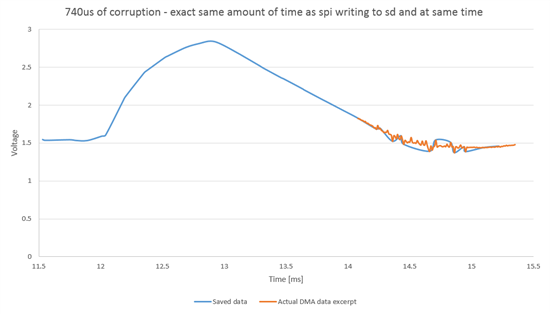
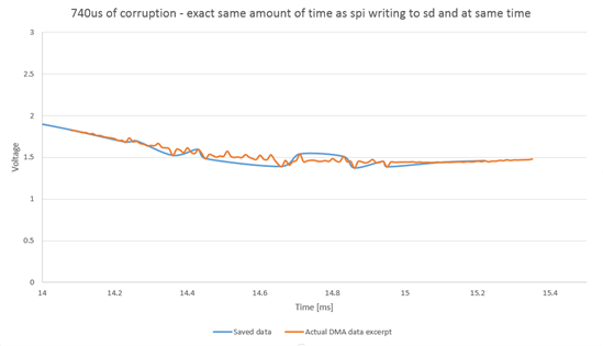
In the images below: The blue shows a data compression of the ADC-measured waveform based on the orange, but it is corrupted during the sd writing (see orange excerpt for the actual high speed ADC data).  The orange is clean on either side of that 700us.

I don't think it's an interference issue on the launchpad because my oscilloscope on the ADC line is perfectly clean and shows where I would expect the waveform to go.

I have also confirmed that the ADC channel integrity is maintained by the DMA, i.e. there isn't any mixing data between expected channels.  

So I am puzzled by this noise which only happens during the time that the SDSPI is writing to the SD card.


ADC channel use:

     ADCSequenceStepConfigure(ADC0_BASE, 0, 0, ADC_CTL_CH0);	    //PE3
	ADCSequenceStepConfigure(ADC0_BASE, 0, 1, ADC_CTL_CH1);	    //PE2
	ADCSequenceStepConfigure(ADC0_BASE, 0, 2, ADC_CTL_CH2);	    //PE1
	ADCSequenceStepConfigure(ADC0_BASE, 0, 3, ADC_CTL_CH3/* | ADC_CTL_IE*/);//PE0 ("P30")
	ADCSequenceStepConfigure(ADC0_BASE, 0, 4, ADC_CTL_CH4);	    //PD3
	ADCSequenceStepConfigure(ADC0_BASE, 0, 5, ADC_CTL_CH5);	    //PD2
	ADCSequenceStepConfigure(ADC0_BASE, 0, 6, ADC_CTL_CH8);	    //PE5
	ADCSequenceStepConfigure(ADC0_BASE, 0, 7, ADC_CTL_CH9 | ADC_CTL_IE | ADC_CTL_END);	    //PE4

SDSPI config:

        SSI2_BASE,          /* SPI base address */

        GPIO_PORTB_BASE,    /* The GPIO port used for the SPI pins */
        GPIO_PIN_4,         /* SCK */
        GPIO_PIN_6,         /* MISO */
        GPIO_PIN_7,         /* MOSI */

        GPIO_PORTB_BASE,    /* Chip select port */ /* Was Port A! */
        GPIO_PIN_5,         /* Chip select pin */

        GPIO_PORTB_BASE,    /* GPIO TX port */
        GPIO_PIN_7,         /* GPIO TX pin */

DMA config:

     uDMAChannelAttributeDisable(UDMA_CHANNEL_ADC0, UDMA_ATTR_ALTSELECT | UDMA_ATTR_HIGH_PRIORITY | UDMA_ATTR_REQMASK);
		//Set the uDMA channel for ADC to be high priority
		uDMAChannelAttributeEnable(UDMA_CHANNEL_ADC0, UDMA_ATTR_HIGH_PRIORITY | UDMA_ATTR_USEBURST/*|UDMA_ATTR_REQMASK*/);
		//Set data size and increment size plus
		uDMAChannelControlSet(UDMA_CHANNEL_ADC0 | UDMA_PRI_SELECT, UDMA_SIZE_32 | UDMA_SRC_INC_NONE | UDMA_DST_INC_32 | UDMA_ARB_8);//arb 4 may cause chans 0-3 to be in positions 4-8 as well
		//Set data size and increment size plus (alternate)
		uDMAChannelControlSet(UDMA_CHANNEL_ADC0 | UDMA_ALT_SELECT, UDMA_SIZE_32 | UDMA_SRC_INC_NONE | UDMA_DST_INC_32 | UDMA_ARB_8);
		uDMAChannelAssign(UDMA_CH14_ADC0_0);	    //Default?
		uDMAChannelTransferSet(UDMA_CHANNEL_ADC0 | UDMA_PRI_SELECT,	UDMA_MODE_PINGPONG, (void *) (ADC0_BASE + ADCSSFIFO0),(void *) (HFS_ADC0_BuffA_Get()), DMA_TRANSFER_SIZE);
		uDMAChannelTransferSet(UDMA_CHANNEL_ADC0 | UDMA_ALT_SELECT,	UDMA_MODE_PINGPONG, (void *) (ADC0_BASE + ADCSSFIFO0),(void *) (HFS_ADC0_BuffB_Get()), DMA_TRANSFER_SIZE);
		uDMAChannelEnable(UDMA_CHANNEL_ADC0);


  • A few questions

    What is your scope time resolution at the time frame you are sampling in? 

    If it's a DSO can you capture sub 1nS spikes on the analog line in single shot mode?

    Do you have a capacitor directly on the A/D input line as close as possible w/o intervening resistor and as little trace as possible?  What kind and what value?

    I have seen A/Ds corrupted by input spikes at much higher frequencies than they can sample at.  High enough that you would conclude the RC filter formed by the S/H circuitry would completely block them.


    Robert

  • snellr said:
    ...during the 700us that the SDSPI is writing to SD, data stored by the ADC and transferred by DMA during those exact times is massively noisy.

    At first read I interpreted this as the data into the ADC - and converted/stored there - did not meet your expectations.  But further reads place this understanding in question.

    Might you define, "massively noisy?"  On any MCU-based ADC - I'd place little faith in the 3 lsb. 

    To gain best performance from our Cortex M4s (this & other makers) we choose MCUs with separate Analog Vdd pins - and employ multiple filter caps and a ferrite bead - at Analog Vdd.  Such can only help.

    I'd repeat your testing with a different maker's SD card - and also insure that during the troublesome SD sequences - your 3V3 and Ana Vdd are stable & noise free.  A current probe's recording of 3V3 draw - during this SD sequence - may also prove useful.  I'd insure that all SD card signal lines are adequate, direct and properly filtered.

    I'm unaware of any other reports of SD card access so plaguing any other MCU peripheral...  And - as always - does this issue arise across multiple boards?  (single board anomaly always subject to, "most anything.")

  • The scope is a "100MHz 1GS/s" Tektronix TDS224 Ditigital Real-Time Oscope.  During the entire waveform, the scope shows a perfectly clean waveform, even during the SD writing.  

    I don't have any caps on the ADC channel right now.  Although that is a good idea, I don't think that would solve this problem because the oscope and the ADC are both sensing the same pin on the launchpad. They produce the exact same values all the time except for during 700us when the sd card writing is taking place.

    I can try putting a capacitor on the pin...

  • Net drops "in/out" my mobile location.  Post may have been missed - arrived few minutes after Robert's. (and perhaps of interest/value)

  • Thanks, cb. I just edited my post to be (I think) more clear.   The scope shows a clean waveform. The ADC data shows a clean waveform everywhere except the timeframe that the sdspi is talking.  

  • Thank you.  Have you scoped the 3V3 and Ana Vdd during the SD transaction period?

    BTW - I'm still unable to understand exactly "what's" been corrupted.  And you've not defined "massively."  (devil may lurk - such details)

  • @cb:  Variation of up to 100 LSB's is shown by the orange data in the graphs of the original post, compared to perhaps 2 or 3 LSB's outside of sdspi writing.


  • It will be the single shot bandwidth that matters not the nameplate bandwidth.  You'll probably need to look at the manual to find it.  Also note that the bandwicth will vary with time scale.  At a slower time scale you will often miss short spikes.

    The capacitor should be size so it is significantly larger than the A/D sampling capacitor and placed only a short distance from the micro A/D input.

    The reason I am pointing this direction is that I have seen (on other A/Ds) a sub ns spike  on an A/D with a slower sampling rate than the TIVA parts cause bad conversions.  The RC formed by the S/H circuit in the micros A/D subsystem would have been slow enough to filter out the spike so it was apparently bypassing the internal filters. These spikes were not visible on the scope except at the very highest speed settings (It's nameplate bandwidth was similar) and even then it was at the limits of detectability. That time division much shorter than you are using IIRC.

    We fixed by adding a small RC (C shorted to input pin) on the input.  On existing boards we patched using 0203 surface mount components.


    CB1's suggestions on power and reference are very good points.

    Robert


    Robert

  • snellr said:
     Variation of up to 100 LSB's is shown by the orange data in the graphs

    I would never have made that assessment - there is no easily readable scale which conveys that fact.  (I'd be curious if Robert was able to interpret such 100 lsb variations - from the 2 graphs you presented)

    Robert's method differs from mine - his belief is that the ADC is prime suspect - mine is that the SD transaction itself will prove the major culprit.  Suspect that Robert's/my ideas - in proper/correct combination - can only improve results...

    Of greatest note - I believe - is your signal management of the SD card's CS pin.  (a small (<100 ohm) series R between SD and MCU is likely to assist.  Might you detail the how/why of MCU -> SD Card signal management?

  • @Robert: I'll throw a cap on (ADC-channel to ground) and retest.  Were you recommending a resistor also?

    @cb: The "100 LSB's" vs "2 or 3" was taken from the source for the graph: Sample provided below:

    Raw ADC @ 100kHz Time (ms) Converted Voltage
    75f 14.62 1.474578755
    7a7 14.63 1.530842491
    75a 14.64 1.470671551
    716 14.65 1.417533578
    6f2 14.66 1.389401709
    750 14.67 1.462857143
    708 14.68 1.406593407
    73c 14.69 1.447228327
    751 14.7 1.463638584
    7b1 14.71 1.538656899
    73d 14.72 1.448009768
    74b 14.73 1.458949939
    753 14.74 1.465201465
    752 14.75 1.464420024
    743 14.76 1.452698413
    743 14.77 1.452698413
    74e 14.78 1.461294261
    742 14.79 1.451916972
    76c 14.8 1.484737485
    747 14.81 1.455824176
    73f 14.82 1.44957265
    78b 14.83 1.508962149
    73c 14.84 1.447228327

    And I'm not sure what you are asking with regard to the SD card signal management.  I chose SSI2 because I was using SSI0 for something else.  The chip select line stays active for basically the entire transaction, but I could try putting a series resistor on it.

  • snellr said:
    The "100 LSB's" vs "2 or 3"

    Clearly - you meant 100 "ADC counts."  After all - ADC is only 12 bits.  I see 6F2 as lowest reading, 7B1 as highest.  that's 191 ADC counts of variance. (between 7 & 8 bits variance)

    Looking at your bulk data - cannot agree that variance is, "massive."  Your "Converted Voltage" tab - portraying 9 decimal point accuracy - is fantasy at best.  And - the 7-8 bit "MAX variation" (again 7B1-6F2) is reported as just 0.149V difference. 

    Your ADC scaling seems "ballpark" (191/4096 * 3.3 = 0.153V)   

    Still - corrective methods presented (Robert/myself) are likely to improve - render your system more robust...

  • @cb: Thanks for clarifying my misunderstanding of LSBs. 

    A 75mV error is unacceptable in my system, and it is much larger than the 2-3mV error during the rest of the ADC sampling, which is why I used the term 'massive'.

    The nine decimal places is just what the excel calculation produced based on the width of the cell, for the sake of creating a graph.

    The ADC scaling was based on a 3.2V reference, which is a reasonable ballpark for the dev I'm doing right now.  I appreciate you bringing that to my attention, though.

    @Robert: Can you suggest a RC adapter to fit between my analog sensor and the ADC pin?  Using just a 0.1uF cap between the pin and ground kills my high frequency data, and further adding a 27 ohm resistor in series between the sensor and the ADC pin also appears to poorly affect the sensor reading.  These are just quick attempts, which I can re-address tomorrow, but perhaps you have some suggestions.

  • A resistor would be good.  A value such that the time constant of the RC is several times the sampling rate. It should not affect your system under ideal conditions but may make more robust to induced noise.

    @cb1 I'm not sure we're that far apart in our assessment, I'm just keying in on the idea that apparently clean data on the scope may not be all that clean if looked at in more detail.  I'm assuming the likely culprit is the SD card interface inducing noise in the supplies or data.  If it's being induced into the ADC module inside the micro there in not much to do other than avoid runnning both at the same time.


    Robert


  • cb1- said:

    The "100 LSB's" vs "2 or 3"

    Clearly - you meant 100 "ADC counts."  After all - ADC is only 12 bits.  I see 6F2 as lowest reading, 7B1 as highest.  that's 191 ADC counts of variance. (between 7 & 8 bits variance)

    [/quote]

    To be fair, TI uses the same misnomer in their data sheets IIRC.

    Robert

  • Believe this horse now dead/dying.  Only thing beyond that past suggested - you may wish to have Excel chart the "delta" - between successive ADC measurements.  It may detect unwanted signal, "swing" upon a certain channel - or due to some other (regularly) repeating condition.  Armed with that (new) knowledge - you may be able to devise further improvements.  (i.e. one channel may be routed in parallel with an especially noisy digital line) 

    You're silent as regards switching & repeating test via different SD card.  And monitoring 3V3 and Vdd Analog both prior to & during the offending time-period.  And the occurrence of this condition upon 2nd, 3rd board...  (i.e. illustrates dreaded, "single board anomaly" vs. an MCU and/or other component-design issue)

  • snellr said:
    A 75mV error is unacceptable in my system, and it is much larger than the 2-3mV error during the rest

    Do you need accuracy or precision?  Right now you appear ot be dealing with precision and repeatability rather than accuracy.

    How fast are you sampling on that channel? You are placing these next to the micro?  Not outside the board?

    Capacitor size should be drive by it's size relative to the S/H capacitor. 10n-100n is usually more than enough.  You may be able to make them smaller.  Resistor choice is then driven by desired bandwidth.  Your worst case scenario here is that the frequency you are interested in measuring and the interfence frequency are similar.  In that case you cannot filter the interference out but must eliminate it. 

    Personally at this point I would not be concerned about distortion.  If the addition of a filter produces a distorted signal that does not show the noise you have previously seen then you have an indication that you may have a noise issue and can then invest in refining the filter.  An issue for which there are people better qualified than I to address.

    Agree with CB1 that you need to measure reference and supply.

    If you need accuracy you will need to address the reference.  Supply voltage is very unlikely to be sufficient.

    Robert

  • I have a list of 8 or 9 items from this post to test today. Will post once I have results. Thanks for the ideas.

  • snellr said:
    I have a list of 8 or 9 items from this post to test today

    If that small - Robert & this reporter must have had, "Off Day."

    Really do urge your scope monitoring of Vdd Ana & 3V3 during "offensive time periods."  And - a 2nd (other brand) SD card could not hurt.

  • Scope BW
    @Robert: I'm not 100% sure about the scope's single shot bandwidth. Having looked at the datasheet, I think it is 0.6ns because... "Delta time measurement accuracy (full bandwidth) in single-shot sample mode: ±(1 sample interval + 100ppm x reading + 0.6ns)" "Sample interval = s/div divided by 250"

    Charting deltas between adjacent ADC channels
    @cb1-:  See attached file for raw ADC values, their deltas, and the graph of the deltas.  Graph does not appear to show any correlation between adjacent ADC channels. Note that the sensor is at rest, no waveform is present so all variation is noise: 3731.Delta file.xlsx

    Swap SD card
    @cb1-: Changing SD card brands made no difference on the amount of ADC-measured noise. (Graph available)

    Apply <100Ohm Res between CS_mcu and CS_sdcard
    @cb1-: Use of 27 ohm resistor as such made no difference in ADC-measured sensor noise. (Graph available)

    Accuracy vs precision
    Currently, I am more concerned with precision--that the waveform matches shape with the waveform I expect.  Eventually, accuracy will become a more significant concern.


    I still have to investigate...

    1. Applying an appropriate RC filter on the sensor output
    2. Scope the 3V3 and V_ana (will try using separate V_ana because right now I'm using the 3V3 on the Launchpad)
    3. Use different launchpad
    4. Ensure sd lines are direct and properly filtered
  • snellr said:

    I have a list of 8 or 9 items from this post to test today. Will post once I have results. Thanks for the ideas.

     
    On our best days, that's what we do.  Spark ideas.
     
    Robert
  • snellr said:
    @Robert: I'm not 100% sure about the scope's single shot bandwidth. Having looked at the datasheet, I think it is 0.6ns because... "Delta time measurement accuracy (full bandwidth) in single-shot sample mode: ±(1 sample interval + 100ppm x reading + 0.6ns)" "Sample interval = s/div divided by 250"

    The important part in this is the very last portion the sample interval. To get a sample interval of < 1ns (necessary to have any reasonable hope of catching nS glitches) you need to have the time scale set to < 250nS/div.  Catching shorter glitches required correspondingly shorter time scales.

    Good oscilloscopes will often (normally?) have anti-aliasing filters to restrict the bandwidth to that that can be reliably sampled.

    Oscilloscopes will often have time scales that need multiple events to see the full bandwidth.  This is fine if the event is repeatable otherwise you will not be seeing a true representation of teh waveform.  You can see that if you capture single shots.  If you are in such a region the display will be only partially filled (every n'th point).

    Robert

  • I didn't see any spikes when I had the scope set to <250ns/div.

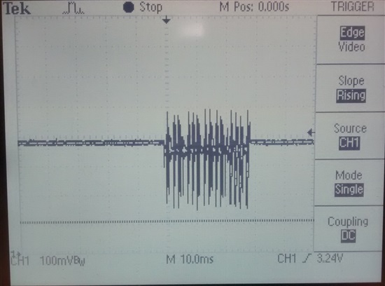
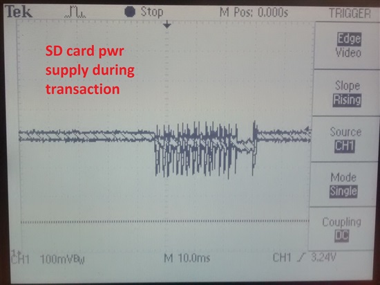
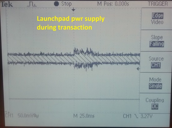
    When measuring the +3.3V on the Launchpad (used for sensor power), though, I did observe the attached picture...  The big noise occurs during SD card writing.  The SD card is on a separate power supply, which also shows the same sudden noise however.

  • snellr said:

    I didn't see any spikes when I had the scope set to <250ns/div.


    That's a good sign.


    snellr said:
    When measuring the +3.3V on the Launchpad (used for sensor power), though, I did observe the attached picture

    OK, now you have a good candidate. Definitely also check your micro's analog supply and reference.  However, even the sensor getting that noise level could be an issue.

    If you have a way to do so you could run an isolated power supply to the SD card (A battery and an LDO?) so you can minimize the disturbance on your main supply. From the looks of things you need a good set of bulk capacitors on that supply.

    I'm assuming the SD card and your main 3V3 share a common source supply.

    Robert

  • These launchlesspads were not designed robustly enough - imho - for such,  (proper) "add-on" accommodations.  Thus was not especially hard for this reporter to make this simple diagnosis (bad 3V3, Vdd Ana) during very first, answering post.

    Proper supplies, signal routings and insurance of proper (common) ground are all required to deliver best signal fidelity.

    This may be the case when a "real" board - with everything properly accommodated - i.e. ground/power planes, proper power and its distribution, and direct/disciplined signal routings pays great dividends.  (i.e. "not" a Launchpad...)

    Such likely, "Loss leader" eval boards surely have their place - but suggesting their "choice & use" for advanced, demanding projects may indicate that vendor's marketing - rather than engineering - won the "naming/labeling" exercise...

  • Further scope shots. SD card on separate power supply:

    Launchpad power supply:

    I still need to put the sensor back in and observe the hopefully reduced noise on the ADC measurements, but I need to leave this for the moment. This is looking promising, though.

  • Thanks to those who contributed to this post.  I'm almost 100% sure that the problem was with the long wires that connected my sd card to the launchpad as well as the long wires that connected my sensor to the launchpad.  EMI. The oscope did not see the noise when I had it on the sensor directly, but when I put it on the mcu-side of the sensor output, the noise appeared.