This thread has been locked.

If you have a related question, please click the "Ask a related question" button in the top right corner. The newly created question will be automatically linked to this question.

TM4C1290NCZAD: EPI Timing issue : EPI Read enable signal delay

Part Number: TM4C1290NCZAD

Hi,

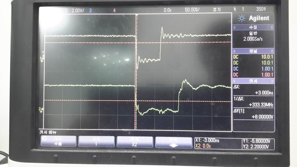
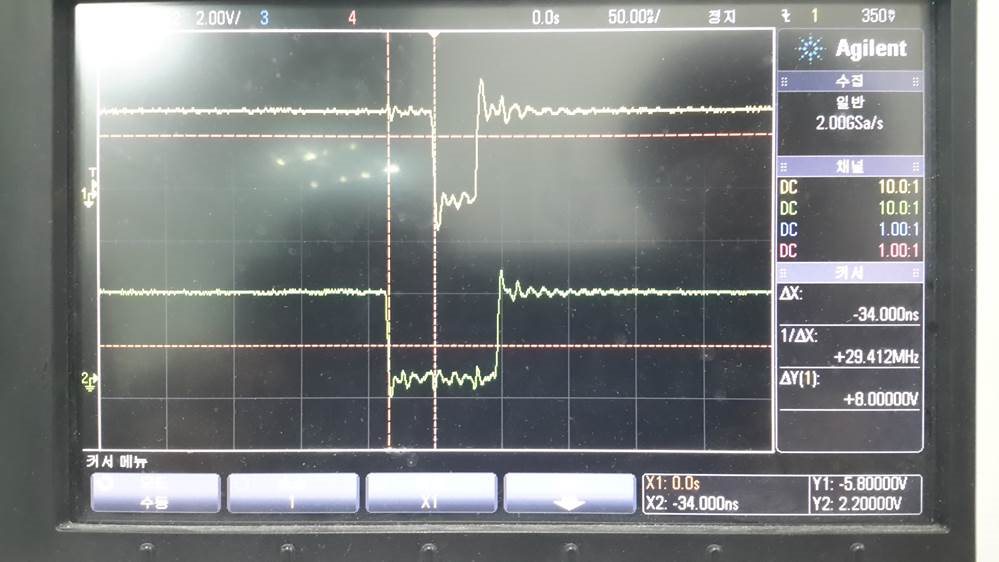
My customer is using EPI Hostbus 16bit mode. when they are writing, CS signal and WRn signal falls simultanously. However, when they are reading, RDn signal falls after one cycle CS falls. Is this normal? What sholud I do to make there is no delay?

Here is the code they used to set EPI:

    EPIModeSet(EPI0_BASE, EPI_MODE_HB16);


    EPIDividerSet(EPI0_BASE, 0x1);


    EPIConfigHB16CSSet(EPI0_BASE, 0 , (  EPI_HB16_MODE_ADMUX             |

                                        EPI_HB16_CSCFG_ALE_SINGLE_CS    |

//                                        EPI_HB16_CSCFG_ALE_QUAD_CS              |

                                        EPI_HB16_BURST_TRAFFIC          |

                                        EPI_HB16_WRWAIT_3               |

                                        EPI_HB16_RDWAIT_3               |

//                                        EPI_HB16_MODE_FIFO              |

                                        EPI_HB16_WORD_ACCESS            |

//                                        EPI_HB16_CSCFG_ALE_DUAL_CS      |

                                        EPI_HB16_CSBAUD                 |

                                        EPI_HB16_CLOCK_GATE_IDLE        |

                                        EPI_HB16_BSEL));

These are timing diagrams for writing and reading

-Writing(WRn - Yellow, CS - Green)

-Reading(RDn - Yellow, CS - Green)

Best Regards,

Ted 

  • Ted Huh said:
    CS signal falls after one cycle CS falls.

    You (likely) meant "RD signal falls after one cycle CS falls."

  • yes. it is my mistake.

  • My interest was one of clarification - saving an extra "back-forth" between you & forum agents.

    Now - firm/I do not use 4C129 MCUs - yet have (long) used external memories tied to wide MCU bus. It is my experience that - most always - both the "WR & RD" strobes must (fully) fit w/in the active time-slot of "CS." With that said - I actually prefer the appearance of the "RD" strobe over that of the "WR" strobe - as the "WR" strobe provides minimal margin to the onset of "CS." (i.e. my group prefers to see such critical strobe signals more "centered" w/in the CS time-slot.)

    In such a situation - I believe that your first (most crucial) obligation is to the satisfaction of the external memory chip's signal timing specification.    Again - our experience reveals that any "simultaneous" signal linkage (likely) violates "set-up" time (in your case) of the external device.

    You may - or may not be able to make some "fine adjustment" of the "time-slot appearance" of those strobe signals from your MCU.  Your (assumed) external memory device is unlikely to accommodate such adjustment - forcing you to choose an external, memory bus device - which well mates w/the MCU's (strobed) time-slot specification...