This thread has been locked.

If you have a related question, please click the "Ask a related question" button in the top right corner. The newly created question will be automatically linked to this question.

TM4C123GH6PM: Custom board design for TM4C123GH6PM

Part Number: TM4C123GH6PM
Other Parts Discussed in Thread: INA219, REF3233

Hello,

I designed a custom board for the TM4C123GH6PM microcontroller. Before doing so, I have carefully browsed this forum, and read the "System Design Guidelines for the TM4C123x Family of
TivaTM C Series Microcontrollers" and the "Using TM4C12x Devices Over JTAG Interface" documents. Before I start the PCB routing, I wanted to the circuit designed to the forum for comments and review.

This design as the usb connector and  we also added a jtag header and connected it to the TM4C123 as shown in the "Using TM4C12x Devices Over JTAG Interface" document. There is also an ideal diode that prevents 5V going to computer side in case external power is used.

Here are some questions I have:

1. Wake is pulled up, or connected to ground? We currently have HIB unconnected and wake is pulled up, and vbat is connected to 3v3

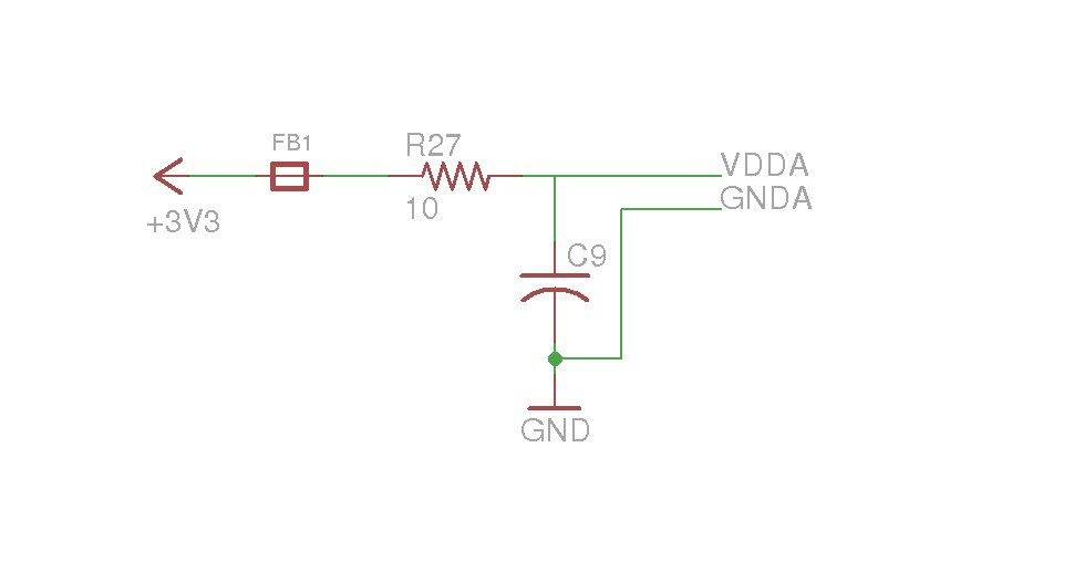
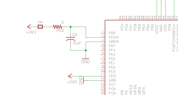
2. Is the gndx connected properly. Some designs connect it to ground.

3. we use PB0/PB1 for usb id and voltage detection. the same pins are also rx1/tx1. This means we can not use those pins as serial?

4. is the RST from the JTAG connector connected correctly? I have the same reset button design as in launchpad, but with the 220 ohm resistor, and jtag reset is connected to IC's reset

Also I am looking for a switching regulator that will take 2S or 3S li-po battery and convert it to 5V@2A-4A - as well as deploy the "Figure 7-2. Using a Crystal as the Hibernation Clock Source with a Single Battery Source" in the TM4C123GH6PM manual with an external battery, and wake button, but maybe thats for another design.

Any ideas/help/recommendations are greatly appreciated.

Best regards,

-Can

  • May I note that yours is a nicely detailed, very well considered post - good job!

    *** for vendor's note ***    Poster's schematic is among the "very few" which appear much MAGNIFIED when clicked to view!    (which then "Opens to new Tab" - renders viewing - SO MUCH EASIER!)    The "loss" of this "Magnification when clicked" appears yet (another) misfortune - caused by the recent forum "alteration" (claimed "upgrade" so highly debated!)

    I've not time now to fully review & comment yet here are a "quick few" which may warrant consideration"

    • it is normal/customary - w/in such schematics - to include a "Notes Section" which guides the pcb assembly process - sometime (even) the pcb manufacture - too
    • VDDA and GNDA appear directly tied to VDD and GND.    While this will work - there is (always) noise upon VDD & GND - and you've imported that (fully) to the Analog Section of your MCU.    This will degrade the Analog Section's accuracy.     It is more normal/customary to employ good filtering of VDD - prior to presenting it to VDDA.    (ferrite bead and small bypass cap - both close to VDDA - improve results - some use a voltage reference - much depends upon your "intended usage" - which has (yet) to be revealed...)
    • it will take both "care & precision" to be able to "Switch both PB0/1 from USB to UART" - suggest you avoid such switching
    • your desire for 2A (especially 4A) @ regulated 5V - from just 2 (especially) or even 3 of your stated batteries - appears "overly-optimistic."
    • as you've chosen "Rechargeable batteries" should not (some) provision for eased "recharging" (either on or off board) "ping your radar?"

    It is wise that you invite comments - prior to such launch.   Extra eyes & ideas - most always - prove of great value.    Points I've listed were, "in my head" - others demand MCU review - outside of my time/effort budget presently...

  • Thank you cb1_mobile,

    The ultimate purpose is to make a general purpose robotics controller board. I intend to keep the design of both software and hardware open, and will be posting schematics at github. Basically, I built a controller for robotics, that talks ROS using the Tiva-C launchpad, and made a circuit for it, and so both the code and the circuit is well tested, and I am making a one board with everything on it. So:

    • I intended to put a voltage reference, although not absolutely necessary would be nice to have. But I could not determine a low cost part for it. I also could not estimate the power requirements for VDDA.
    • So, it is problematic to switch PB0/1, this is ok, because we still have other serial ports.
    • About power, my board will be using maybe 1.4A max. But there are also plans to back-power a RPI from this board, which would require an extra 2.5A for the RPI. But I now see, it is over-optimistic. The most important thing about this power supply is that I need low noise pass through.
    • A battery charge/monitor circuit would be superb. I have an INA219 doing this in the previous version of this board, for current and battery monitoring, but we never came to that part.

    Thank you.

  • Thank you - as such application would benefit from "improved ADC performance" your routing of VDD through small value series R (<10Ω) w/that resistor in series w/ "small ferrite bead" and the bead bypassed by small value cap. (w/both bead & cap very close to VDDA) will raise ADC performance.

    You may tie GNDA to board's central GND (at one point only) - you do not want GNDA to "run in series w/digital GND." (which carries high current - thus will change GNDA's level.)

    While it is unlikely that you can "add a (proper) charger circuit now" - it would prove an advantage if you could provide means for such "charger" to "easily & correctly" (and ONLY) plug-in properly - to "Speed, Ease & Enhance" battery charging.    Ideally you'd be able to (both) operate the board AND charge the battery - while powering from the "charging source."

    Note too - there should be an "on-board means" to measure battery's "current state of charge" - which sounds an alert - when charging is becoming needed/helpful.    (i.e. just as is done in a "real" product...)

  • Hello,

    So I draw a circuit to illustrate the ferrite bead: [routing of VDD through small value series R (<10Ω) w/that resistor in series w/ "small ferrite bead" and the bead bypassed by small value cap. (w/both bead & cap very close to VDDA)]

    I am not sure about the bead being first or the resistor connected to 3.3V

    Also, I have been meaning to put a REF3233 to do the job, but I am not sure if 100uA will be sufficient.

    Best regards,

    C.

  • As the ferrite bead presents (some) inductance - it usually mounts as close as possible to pin VDDA. Note that the bypass cap - and possibly a small filter cap (10µF) in parallel - appear across VDDA & GNDA - yet GNDA should join to the board's main GND (at one point only) - and not carry the (far larger) digital GND currents. (you must not sacrifice "routing ease" for Analog performance.)

    MCU manual (far back in the rear (specs) ) should reveal the current demands placed by VDDA. Like you - I don't believe the "reference value" you note proves sufficient - your directed search should reveal/confirm...
  • can altineller said:
    I intended to put a voltage reference, although not absolutely necessary would be nice to have. But I could not determine a low cost part for it.

    What do you consider low cost?

    https://www.digikey.ca/short/qtqhtr

    starting at < $1 ea./C

    can altineller said:
    The ultimate purpose is to make a general purpose robotics controller board.

    Considering this and that you are using a battery pack. Assuming you are only using a single battery pack for the robot power and the micro to avoid the complexities of independent battery packs you need to take some precautions on the power

    • Use a diode from the battery to you DC/DC. This is for two reasons
      1. you don't drain the voltage from the micro in order to run the robot during high power surges
      2. you don't end up with a reverse voltage across your regulator, some fare badly if the output voltage is greater than the input
    • Use a substantial capacitor on the input to the DC/DC. This is to help ride through lowvoltage events from power surges.

    Robert

  • Hello, I have checked the power consumption of VDDA (denoted as Idda) and it is around 5mA. most of the voltage references are microamps, and a solution like MAX6071 (10mA output) costs > 3$.
  • Friend Robert has made several highly valuable suggestions - you should read/review & comment.

    Should not "low cost" be very second to, "remain working - w/most "reasonable" performance?"

    High volume (i.e. consumer devices) surely must minimize cost.    Your targeted design falls far from that - robustness & adequate performance (demanding some cost) - would prove far more, "expected & desirable" - in my opinion...

  • can altineller said:
    Hello, I have checked the power consumption of VDDA (denoted as Idda) and it is around 5mA.

    Using a reference as a power supply is probably not a good idea, they are quite different functions.

    VDDA should be driven from a separate source than your reference input.

    Robert

  • Thank you Robert,

    I understand VDDA is not a reference input, but power input to analog circuits on the chip. Although the max current for VDDA is 5mA, something could go wrong and temporarily consume more, and drain the voltage reference right?
  • Hello cb1_mobile:

    I decided not to employ an a reference but feed the VDDA with the ferrite bead. However, being inexperienced in this, I could not really picture the circuit you mentioned. And I also have no idea what values to pick for the ferrite bead, the resistor in series, and the capacitor.

    Is the circuit I draw above (the one that depicts the ferrite bead) correct? I am confused about whether the resistor or the ferrite bead should be connected to 3.3V?

    Best regards,
    C.
  • I'm confused - have you not "self-awarded - Issue Resolved" (upon your post, immediately above?) Thus all new visitors to this thread simply, "Click till they reach "Resolved Green" - and then - the clear "solution" lies before them.

    How could you conclude to award "Resolved" - when that post is almost entirely, "questioning in nature?"    (thus clearly - fails to resolve!)    

    BTW - I've earlier listed connection detail - & many part values - simply search among the "Better Resolving - yet award-free" earlier postings...

  • can altineller said:
    Although the max current for VDDA is 5mA, something could go wrong and temporarily consume more, and drain the voltage reference right?

    No. There are several issues.

    The drain is variable so the supply has to react to that. Note too that this can have quite a frequency spread, from the possibly quite slow demands of the conditioning circuitry to the high speed operation of the SAR and the charging and discharging of the comparison capacitors.

    Power supplies have a droop, so even for slow demand changes the output will vary, although for small changes they will not change very much. This is actually fairly important to their regulation.

    References on the other hand are designed to feed inputs that are high impedance and to maintain accuracy over temperature.

    Basically references and supplies are designed for different purposes and are not well suited to the other's purpose.

    That said, it's not necessarily a problem. Many sensors are ratiometric, that is their output scale changes with the power supply so a sensor with a 3V output on a 5V supply will have a 1V8 output on a 3V supply provided both voltages are within its range. In that case as long as the sensor and the A/D share the same supply as reference then the conversion is insensitive to the accuracy of the supply voltage/reference. In that case separating the reference and supply actually results in worse accuracy.

    Robert

  • Well, it was a mistake. I somehow thought clicking "this resolved my issue" was like clicking "like".

    Is there anyway to undo it?
  • can altineller said:
    Well, it was a mistake. I somehow thought clicking "this resolved my issue" was like clicking "LIKE".

    Superior (in their minds) intellects (i.e. forum mgmt) have declared "LIKE" as unnecessary (which is so very mistaken) - thus contributing to your issue.

    Indeed - their most recent (claimed - yet highly debatable) forum "upgrade" has removed the opportunity to "reverse a (mistaken) "Verified/Resolved.""

    Might we need, "Saving" - from those who claim to, "Save us?"

  • Well, running a forum this big could bring challenges. Is this a custom developed forum or a 3rd party software?

    I guess it still allows me to pick another post as `this resolved my issue` because they are still green.

    As to the ferrite bead I have drawn something like this:

    I also found ferrite beads that are 805 packaging. They have values like 60R 100R. I have done extensive googling to figure out what the value of the ferrite bead should be in this type of circuit, but I was not able to conclude a value.

    best,

    C.

  • Removing the "sure motivational benefits" afforded by "LIKE" should present NO challenge!     It was - may I state - simply (beyond) "dumb/misguided!"    (as I've past co-founded - drove tech start-up from zero to 17M (USD) w/in 4 years - and then taken firm PUBLIC - it might just be that I am "qualified" to "argue for LIKE!"

    It has become true that, "More answering/responding posts" are generated by we "outsiders" than captive vendor staff. (show up here on a weekend - when the ratio (easily) exceeds 10:1 - favoring outsiders) Thus - to remove motivation/earned affirmation - from one's peers - makes NO sense!

    I did note that the ferrite should be placed close to the MCU VDDA pin, its series resistor ties to VDD - should you choose such approach. W/in that same post (BTW - I've not noted it "Green") part values (typ.) for bypass & filter "Cs" were (also) presented. Those beads are inexpensive - you'll do best to order small quantity of multiple values - each circuit is unique - identifying a "universal value" is unlikely. (resistance of the bead (and any series R) should be low enough that the "maximum current draw of VDDA" does not cause VDDA to "droop." (you can use that guide to perform "first order calculations - then choose ferrites which "bracket" that value. (say ±30%)

    Your latest schematic has missed a small value, bypass cap - emplaced (right at) VDDA. Again that guidance - and value - appeared in a past (still non-Green) posting...

  • Hello,

    I have been searching for the past post you mentioned, but I can not find it. Maybe there are some other issues with find-ability? I also checked your previous post, but was unable to find.
  • cb1_mobile said:
    application would benefit from "improved ADC performance" your routing of VDD through small value series R (<10Ω) w/that resistor in series w/ "small ferrite bead" and the bead bypassed by small value cap. (w/both bead & cap very close to VDDA) will raise ADC performance.

    Above w/in Sat, 21 Oct, 11:47 posting (this reporter)

    And ... same date, 1:07 

    "...ferrite bead presents (some) inductance - it usually mounts as close as possible to pin VDDA.    Note that the bypass cap - and possibly a small filter cap (10µF) in parallel - appear across VDDA & GNDA."