Hi all,
I have been working on DRV8301 reference design given in figure 7 of datasheet. I have developed circuitry as show in the design and I have disabled buck converter by driving EN_BUCK LOW and also by removing 22 uH inductor and 47uF capacitor on PH pins of the IC. After that SPI communication works and I observe some output at GX_X pins of the DRV8301.
I have checked voltage at different pins and it is correct as per the datasheet, GVDD = 11V, AVDD = 6.3V, DVDD = 3.3V, BST_A = BST_B= BST_C = 11V. PVDD1 = PVDD2 = 26.1V.
Also SPI registers do not show any faults and their readings are as follows,
Register Value read
0x00 0x0000
0x01 0x0801
0x02 0x1400
0x03 0x1800
As per the datasheet these read values do not show any error or fault condition. I see that PWRGD = 0V and nOCTW = 5V and nFAULT = 2.3V.
I believe PWRGD = 0v is indicating buck disabled and nOCTW is correct and nFault also seems correct.
Now I have not connected any MOSFET circuitry, so there are no connections on pins 30 to 48 to MOSFET circuitry. This is because I just want to observe DRV8301 PWM output first before driving MOSFETs.
But no matter what is applied at the input of INX_X pins of DRV8301 I get some square wave output smaller than 5V at the output of GX_X pins. This is weird and I have been working for more than 2 weeks with no luck. All voltages and SPI registers are normal and show no indication of fault or error. But then why PWM output is not available as it is supposed to?
But then why PWM output is not available as it is supposed to?
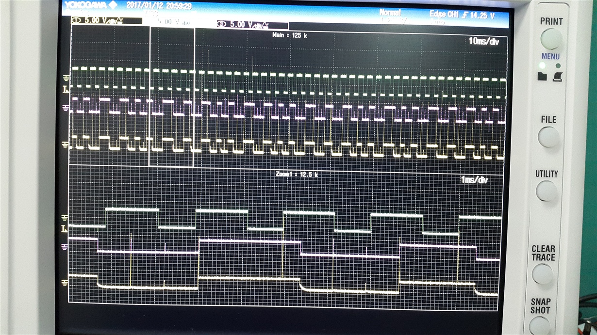
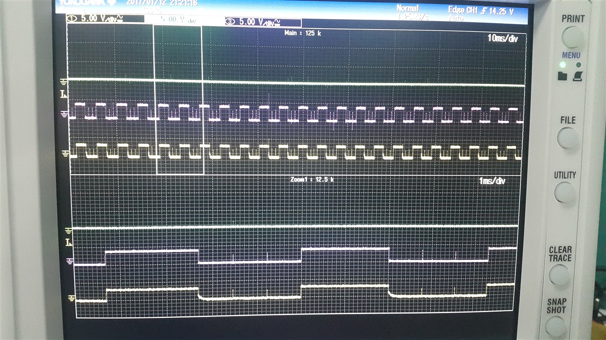
Attached are figures showing capture of pins INH_A , GH_A and GL_A waveforms in the same order.
First waveform is INH_A, second is GH_A and third is GL_A.
First half of the screen shows waveforms in not zoomed in and lower half shows waveforms zoomed in by 5X. Even after having valid PWM input at INH_A, INL_A, GX_A do not show required output.
With PWM at INX_A
Without PWM at INX_A


