This thread has been locked.

If you have a related question, please click the "Ask a related question" button in the top right corner. The newly created question will be automatically linked to this question.

DRV8323: DRV8323RS VDS_OCP failure

Part Number: DRV8323

Hello,

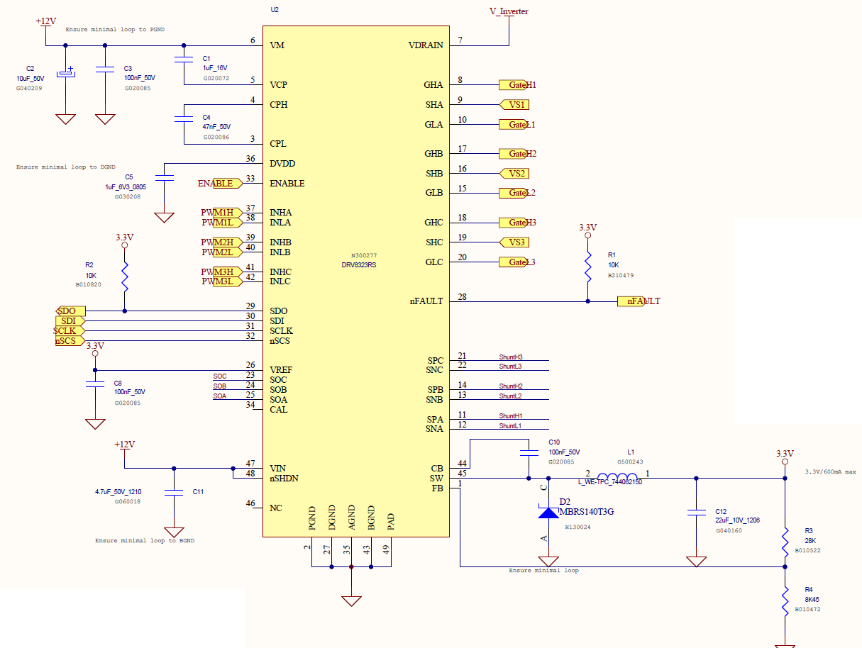
I use DRV8323RS on my design for motor control, and I have some problem due to failure on VDS_OCP.

I validate SPI communication to configure this driver and com works well without any errors. To know my configuration here are the values of registers :

Register 0x02: 0x1000

Register 0x03: 0x1BFC

Register 0x04: 0x27FC

Register 0x05: 0x2B52

Register 0x06: 0x32C3

After that I wanted to test the driver output with some TTL signals. For example I put high the signal INLB to obtain a high output signal in GLB (low side mosfet of B half bridge). The others inputs of drivers are set to zero. When I implement the code on microcontroller I get failure data on Register 1 (Address 0x00). The following bits are activated: FAULT, VDS_OCP and VDS_LB. It detects VDS overcurrent but there is no current consumption on the power supply.

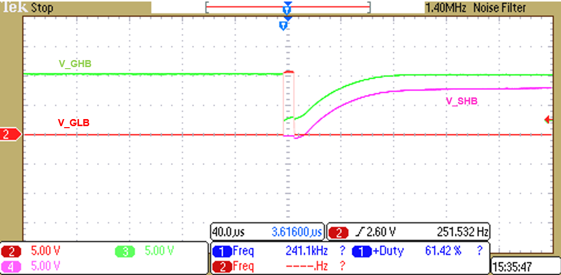
Moreover I observe on mosfet of high side that there is 11V on each gate without request from microcontroller (maybe a specific behavior but I never see it with other mosfet drivers). You can see schem3 picture in attachment file with V_GLB V_GHB and V_SHB signals when failure occurred.

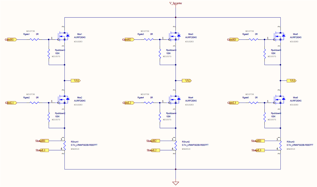
The picture schem1 and schem2 are schematics of power stage.

I don’t know if it’s clear, but if you have any idea or advice don’t hesitate to share with me.

Thank you a lot for your help.

Regards,

Samy

Schem1

Schem3

  • Samy,

    Let me try to understand your setting first:

    Register 0x02: 0x1000;   Binary: 0001000000000000b; Default setting: xxxxx00000000000b;

    Register 0x03: 0x1BFC   Binary: 0001101111111100b;Default setting:  xxxxx01111111111b; change IDRIVEN_HS from 2A to 1.14A

    Register 0x04: 0x27FC    Binary: 0010011111111100b;Default setting: xxxxx11111111111b; change IDRIVEN_LS from 2A to 1.14A

    Register 0x05: 0x2B52    Binary: 0010101101010010b;Default setting:  xxxxx00101011001b; change dead time from 100ns to 400ns; change VDS_LVL from 0.75V to 0.2V

    Register 0x06: 0x32C3    Binary: 0011001011000011b:Default setting: xxxxx01010000011b; change current sense gain from 20 to 40

    Next time, if you can give the setting changes and purpose from your description, that could speed up the debugging. Please confirm those changes, I will get back to you ASAP.

  • Hello,

    Thank you for your quick reply.

    Sorry next time I will detail more my configuration. 

    All your comments of my register modifications are good.

    Regards,

    Samy

  • Samy,

    From the schematic, "+12V" and "Inverter" are on different net.  To debug this:

    1. Can we connect  "+12V" and "Inverter" together? Are "+12V" signal and "Inverter" signal independent?

    2. When  "+12V" and "Inverter" are separated, the  "Inverter" doesn't have any capacitors to hold the voltage stable. Can we add same capacitors as "+12V" has?

  • Hello,

    I connected « 12V » net and “V_Inverter” net together but the driver behavior is not changed.
    I tested my software with a BOOSTXL-DRV8323Rx, and the driver outputs generate good signals from INHx/INLx (with good voltage level: GHx=23V with VM= 13V). And without any error on registers 0x00 and 0x01.
    I checked the BOOSTXL-DRV8323Rx design on Altium and I don’t see additional capacitors on VDRAIN to hold the voltage stable (when VM=VDRAIN, as my design when I connect 12V and V_INVERTER together).
    I don’t know if a failure on boostrap capacitor can cause this driver malfunction.

    Thank you for your support.

    Regards,
    Samy
  • Samy,

    OCP circuit senses VDS voltage and compares it with V(VDS_OCP) setting. When we have OCP issue:
    a. Check VDRAIN pin has Kelvin connection to the FET's drain.
    b. Make sure a capacitor between high side FET's drain and low side FET's source.

    To debug this, can you set different V(VDS_OCP) trip points, do you see any difference?
  • Hello,

    There were some mistakes during pcb design, I noted that there are no links between SHA SHB SHC and sources of high mosfets. When I connected these elements errors on SPI bus have disappeared and driver outputs are now correct.

    Thank you for your help.

    Regards,

    Samy