This thread has been locked.

If you have a related question, please click the "Ask a related question" button in the top right corner. The newly created question will be automatically linked to this question.

DRV8323R: IC Fails occasionally with gate drivers shorted

Part Number: DRV8323R
Other Parts Discussed in Thread: DRV8323,

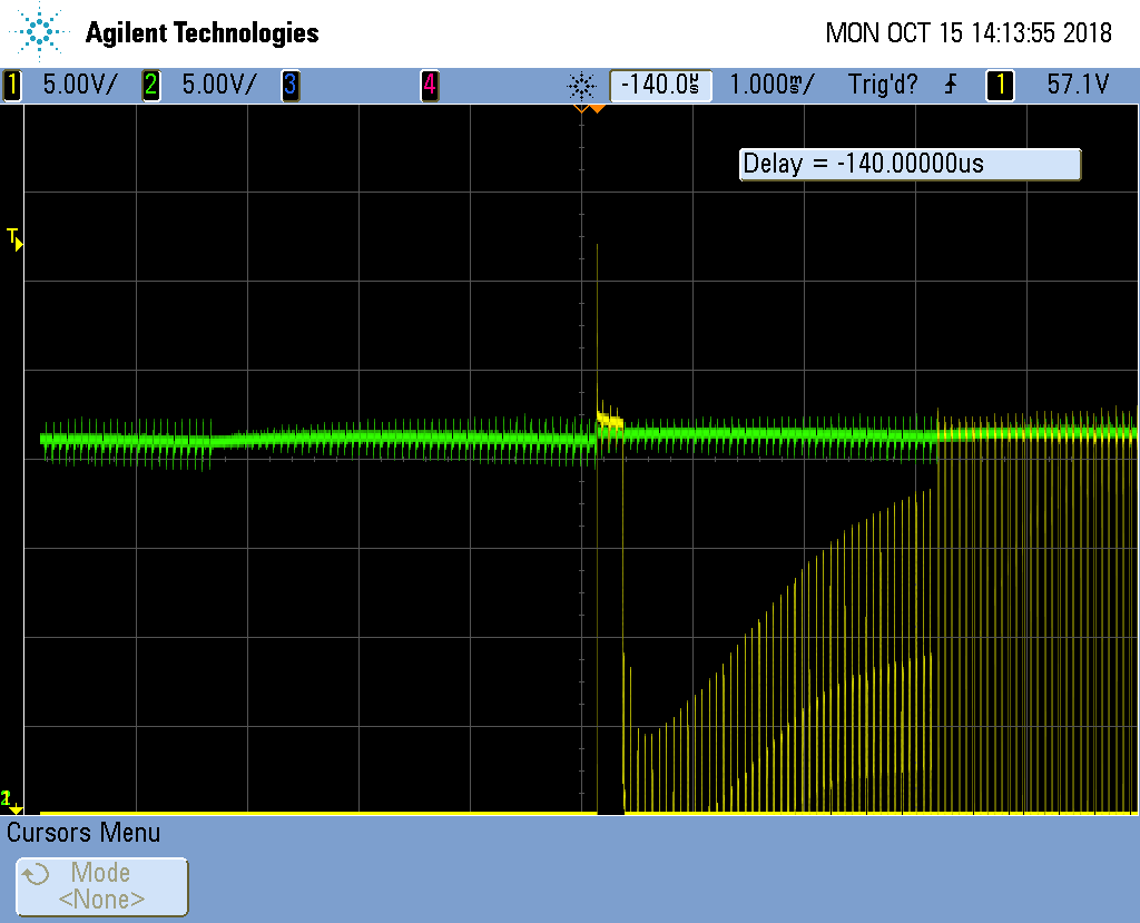
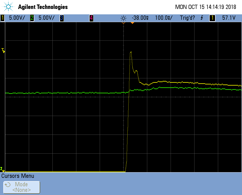
We have a design using the DRV8323 that has been working great but every once in a while the DRV8323 fails with all the fet gate drives shorted.  The Mosfets are fine!  The etches to pins 7 (VDRAIN), 8(GHA) and 9 (SHA) get blown off the PCB making the board un-repairable.  The PCB layout was taken from the App notes and Data sheet.  The pcb copper is 2oz.  The board temperature by the DRV8323 is 50C. We use it in PWM x 1 mode, supplying a 15KHz signal.  The supply voltage is 48Volts and has a large snubber to keep the supply to less than 52 volts (measured) during a back EMF event.  The motor is rated for 500 watts. The internal switching power supply continues to operate properly!  Please advise

  • David,

    Would you verify it with an EVM?
    I am thinking the a over voltage stress kill the part. So, please check how much capacitance do you put on VTM and VDRAIN?
  • I don't have an EVM. Your analysis sounds correct but I have been unable to capture the event on a scope. There is a bulk capacitance of 3 x 6800uF caps on the 48V supply about 50mm from the IC. There is a 1uF (C18) on the VM pin to The VCP  <3mm from the IC.  There is a .1uF 100V (C23) ceramic cap < 6mm from the VM pin to the power ground plane which is also connects directly to the power pad of the DRV8323.  There is a 10uF  (C25) 100V ceramic about 25mm from the VM pin to the power ground plane also.  The VDRAIN pin connects directly to the  DRAIN of one of the mosfets just like it's shown in Figure 64 Layout example in the data sheet with NO capacitance. Should there be?.   The design uses a split plane as shown in SLVA951 "Figure 9. DRV8323R Split Ground Plane".  The two grounds are tied about 7mm from pin 1 of the IC as shown in Fig 9.   When the motor is "free wheeled" I get a peak voltage of about 52 volts on the 48V buss.

    Top Layer (Pink) and 2nd layer showing connection from VM pin to drain of MOSFET and VDRAIN to Mosfet Q27 Top layer with ground plane, power ground to logic ground is tied on the green layer between the C20 and C19 reference designation silkscreen  underneath the pink etch.

  • David,

    What Csw (the capacitor between CPL and CPH pin) voltage do you use? That capacitor voltage rating should have VM-rated capacitor.
    Also, I would put few VDRAIN capacitors near the switching FETs (from top FET's drain to bottom FET's source or current sense resistor ground).
  • I have a 0.047uF 100V ceramic from CPL to CPH.  I have 2.2uF 100V ceramic in parallel with 0.1uF 100V cermaic size 1812's in locations C6, C26 and C4(not in view) stacked on top of each other from each of the mosfet drains to ground right by the Rsense resistors R23, R27 and R5(not in view).  Are you suggesting they should go to the mosfet source / Rsense junction not ground?  

  • David,

    The VDRAIN capacitors are stacked from each of the mosfet drains to ground right by the Rsense resistors R23, R27 and R5(not in view). That is correct.
    Do you see any abnormal voltage on VM; VDRAIN; GHA and SHA?
  • I have only monitored the 48 volt supply at the bulk capacitors.  It goes up to 52 volts when the motor free wheels.  I will monitor VM and Vdrain right at the pins.  Should I use a diff amp to monitor the GHA to SHA  or are you looking fo the absolute voltages?  What should I use for a ground pin reference for the scope? pin 2?  Thanks

  • David,

    You can monitor them (VM; VDRAIN; GHA and SHA) in a same scope different channels. Set GHA voltage as a trigger source to catch the failure event (Normal trigger on GHA). In that moment, we can check which one go crazy first. Or if the abnormal voltage shows up early before the damage, we may find the root cause before the damage.
  • I started off by monitoring the VDrain and SHA pins.  I found when I quickly change the PWM from say 60% to 10% duty I get a spike of about 58V at SHA when commuting occurs.

    The spike is very short. 

    I have a snubber from the drain / source junction of the fets of 4.7ohm in series with 4700pF.   This spike only occurs when I change the PWM quickly.  The VDrain pin has no spikes on it that I've been able to detect.

    Please advise.  Thank you!

  • David,

    You said, 58V. But, the yellow probe has 5V/div.
    1. For a buck converter, if a duty cycle is suddenly reduced, the energy will send back to input. The converter runs from buck mode to boost back mode. SHA voltage is higher than VDRAIN. I would think the energy is sent back when you change PWM quickly.
    2. High side FET's body diode should connect SHA to VDRAIN bypass capacitor. If they voltage difference is much higher than a diode drop, I would think too much parasitic inductance between SHA to the VDRAIN bypass capacitor. Would you add a local capacitor between high side FET drain and nearby power ground.
  • Thanks for your quick reply

    The scope has an offset of 45 volts putting the center line at 45 volts.  The trigger point (upper right hand corner) is 57.1 volts.  This is still below the 65 volts Absolute max but I'm guessing there must be some point it shoots higher causing the failure.   It typically takes days before I get a failure.  I added 10uF 100V Ceramic SMT across location C26 which is the closest I can get physically.  The ground is right at the current sense resistor and right at the drain tab of the high side mosfet.  The spike amplitude did not change.  I used one of our "solder inplace" scope probes to eliminate ringing to make the measurements.  Is it possible this could be turn on time of the fet body diode?  I always thought it was in the order of ns and nobody ever gives a spec for it.  Is there another way you could suggest?  Would a small rc in series with the SHA pin help?  TVS? 

  • David,

    Before talk about solution, we have to find the root cause first. The waveform is same after you added 10uF ceramic capacitor. That is a little bit surprise to me. From the schematic, only one FET is between SHA and that capacitor (please help me confirm that). But, if it is true, that tells us:
    1. 10uF is much less than what you have there. This is not true, right?
    2. The FET path has a very high parasitic inductance.

    Please also double check your probe ground connection. Don't let ground current di/dt give a measurement error here.
  • Answers to your questions:
    1. Each 1/2 bridge of fets has 0.1uF & 2.2uF from +48V to gnd right at the fets. See C6 and C26 above. The ground is 2 layers of 2oz copper that is right under the fets. There is also 3 x 6800uF bulk storage 40-50mm from the 1/2 bridges. So my guess would be that placing a 10uF cap across the 2.2uF/0.1uF pair would not do much which agrees with what I measured.
    2. The fet case package is a TO263-7. Infineon pn IPB180N08. They don't give an package inductance.

    I have used a probe from a diff amplifer for making the measurement. It is soldered in place right at the pins with less than 12mm unsheilded. With such an extremely fast spike I can see your point here. Do you have another sugestion? The scope is a 2Gs/s 100MHz.

    Thanks
  • David,

    If the measurement gives us the true info, next step we check: does TO263-7 package inductance or lead parasitic inductance cause the issue:
    a. can you slow down the low side FET turn-on speed? It can slow down the di/dt transfer from low side FET to high side FET path.
    b. can we change the FET to a small package (such as TO220) and short the lead wire to verify the parasitic inductance factor.

    I would think the item a could be a potential solution.
  • Hello

    I used anther scope and probes to verify the waveforms I was measuring.  Both scopes have similar wave forms but the second scope the spike voltage was 2-3 volts higher.  The BW limit was on in the first scope.

    I don't see how to just change the low side mosfet turn on time (I'm not using the spi bus) with out adding a gate resistor/diode. I tried lowering the gate drive current from an iDrive Resistor value of 18K to infinite.  (570/1140ma down to 120/240ma)  The spike drops 4-5 volts so it has gone from low 60s to high 50s volts.  The board runs a few degrees warmer.  What is a safe limit?  Should I try a gate resistor and diode?

    Thank you

  • David,

    Yes. Change gate drive current setting can change the low side FET turn-off speed which can reduce the voltage spike.
    But, we just want to eliminate the spike. The spike energy should not bring the whole board few degree warmer. If it does bring few degree warmer, we may slow down too much.
    If the TO263-7 FET current path has a very high parasitic inductance, can we add a schottky diode parallel with it (directly from the load to the 2.2uF or 10uF ceramic capacitor?
  • Hello

    I ordered some schottky didoes.  I also looked for a negative spike below ground and see a -5V spike in the 20ns wide range.  Should I also put diodes to ground?

    Thank you!

  • David,

    Yes. Please also put a schottky diodes from switching node to ground. This is on debugging stage. It won't hurt to find the root cause.
  • I added in the schottky diodes as you suggested.  The spike dropped again but was not eliminated.  I lowered the gate drive current again, which seems to have the biggest impact.  I have been running the system now for days starting and stopping the motor quickly and changing speeds with no failures.   I removed the schottky diodes and have again have run the motor for days monitoring for spikes and have not seen any spikes greater than 2 volts over the power supply.  Comments?

    Thanks

  • If the gate drive current control can eliminate the switching spike, you may not need the schottky. Adding schottky just tries to provide another current path besides the high parasitic inductance switching FET path.