This thread has been locked.

If you have a related question, please click the "Ask a related question" button in the top right corner. The newly created question will be automatically linked to this question.

DRV8702-Q1: IN2/EN affects IN1/PH

Part Number: DRV8702-Q1

Hello community

I have a DRV8702 running in independent half-bridge mode. When I drive the input IN1/PH the motor connected to half-bridge 1 is working as desired and the motor on half-bridge 2 is off.

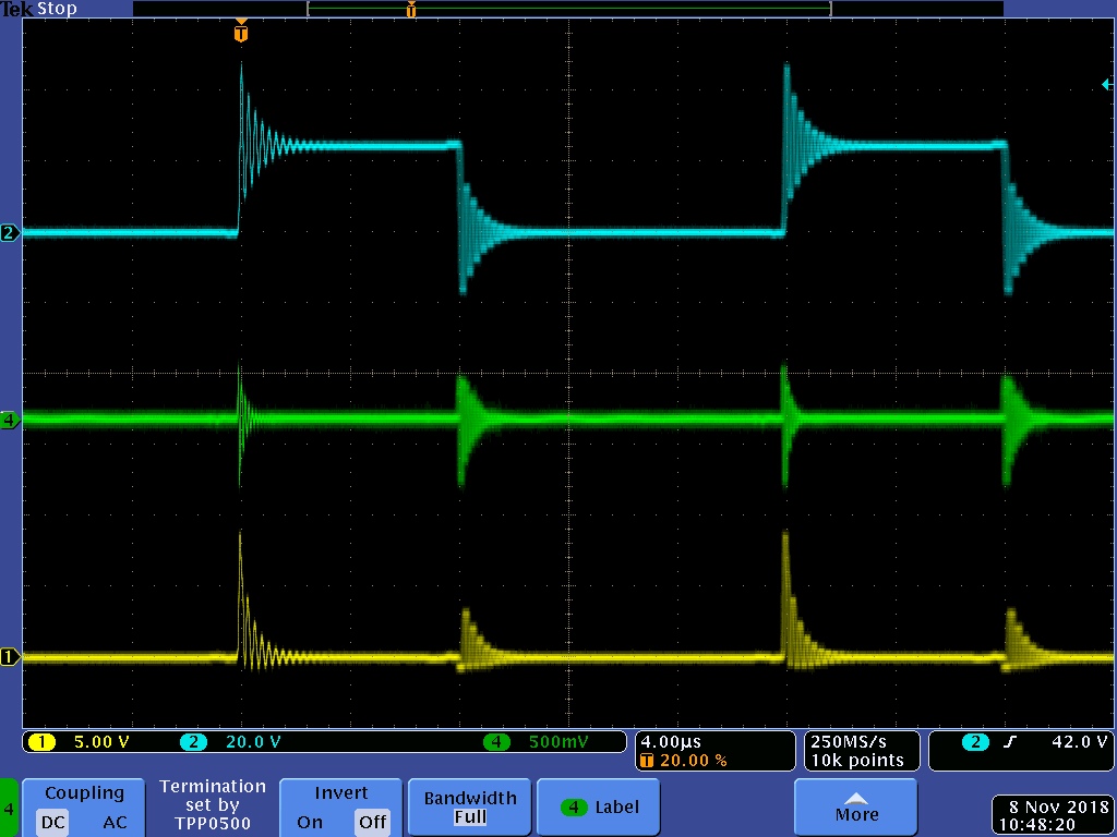
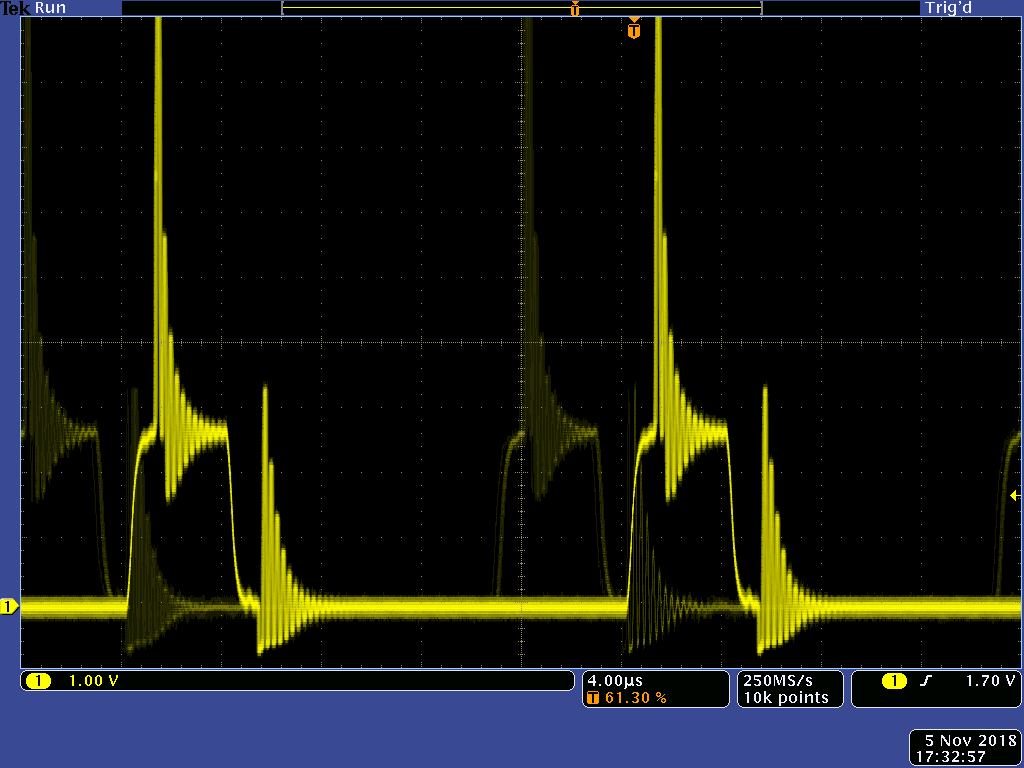
When I drive the input IN2/EN the motor connected to half-bridge 2 is working but the motor on half-bridge 1 also makes some noise and the temperature of the DRV increases for about 15°C compared to driving the input IN1/PH. The following measurings show the problem.

Here is my circuit and the measurements:

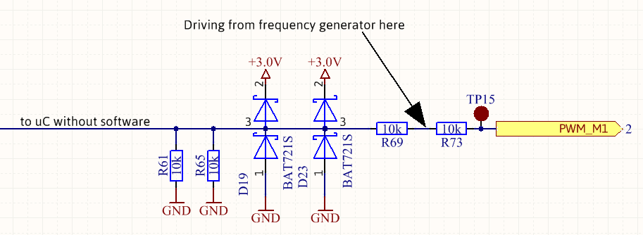
Circuit for PWM_M2 is exactly the same as above.

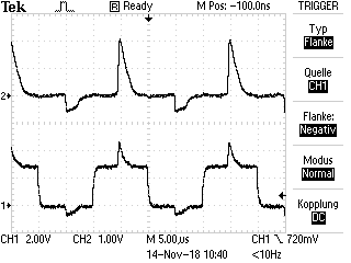
Driving IN1/PH / Measuring IN1/PH --> OK

Driving IN1/PH / Measuring IN2/EN --> OK

Driving IN2/EN / Measuring IN1/PH --> NOT OK

Driving IN2/EN / Measuring IN2/EN --> NOT OK

I have the same problem with multiple boards.

Do you have any ideas why this could happen? How can driving IN2/EN cause such a signal at IN1/PH?

Thank you for helping

  • Hi Robin,

    Try connecting the MODE pin directly to DVDD with a 0-0hm resistor rather than through a 10 kOhm resistor. The mode pin is designed to sense a Hi-Z state using an internal voltage divider, and sometimes noise can impact the internal node voltage if there is an external impedance. Figure 32 in the datasheet shows the circuitry on the MODE pin.

  • Hi James

    Thank you for your reply. I already tried this but it didn't work. Even with the 10k resistor the voltage at the pin is much higher than 1.35V which is needed.

    Any other ideas?
  • Robin,

    I'm reviewing your scope shots again, and I don't think think that the IN2 signal causes this ringing directly. Since the ringing is on both inputs, this means that something else is causing it. If you measure both INx pins at the same time, I think they should both ring at the same time. My first guess is that this might indicate ground bouncing due to some kind of parasitic impedance on the output stage traces. You may want to double check any differences in routing between your two half bridges that might cause ringing when IN2 switches.

    To debug this, can you try a few things?

    1) Remove the load from the FETs so no current flows. Do you still see the ringing on the inputs?
    2) Replace your sense resistor with a 0-ohm resistor or a short and recheck if there is ringing.
    3) Measure the nets around your FETs with an oscilloscope. There may be some parasitic impedances caused by a difference in routing that causes one output to ring while the other one does not ring.
    4) Measure the ground pin on the DRV8702-Q1 and on the low-side FET connected to GL2. Reference your probe to a quieter ground by connecting it directly to the supply ground.

    Since the gate drive device gets hot, it is possible that it may be damaged. The voltage of the ringing violates the absolute maximum ratings of the device.
  • Hi James

    Thanks again for your response.


    1) Remove the load from the FETs so no current flows. Do you still see the ringing on the inputs?

    --> Done, no changes

    2) Replace your sense resistor with a 0-ohm resistor or a short and recheck if there is ringing.

    --> Done, no changes

    3) Measure the nets around your FETs with an oscilloscope. There may be some parasitic impedances caused by a difference in routing that causes one output to ring while the other one does not ring.

    Blue: Output X5, Green: Source of FET Q10, Yellow: IN1

    4) Measure the ground pin on the DRV8702-Q1 and on the low-side FET connected to GL2. Reference your probe to a quieter ground by connecting it directly to the supply ground.

    Blue: Source at FET Q10, Yellow: GND at DRV

    As you can see the ringing is on every signal I measured including the motor output. But the ringing on the GND pins can be measured also when driving input IN1. But I think the difference between the inputs is as you said the layout.

    IN1 drives the bridge on the left, IN2 drives the bridge on the right. Layout is more or less identical. But as you cann see the traces for IN1 and IN2 (highlighted in blue) are routed under the output of bridge 2. I think the ringing of the output signal (blue signal on first pic) couples into the IN1/2 traces and causes the problem.

    So I see two possibilities: Prevent the output signal from ringing or improve the layout (will be done for sure for next prototypes).

    Do you have an idea how to reduce the ouptut ringing or is this normal?

    Thank you for your help.

    Best regards

  • Robin,

    It is definitely possible that the ringing on the outputs is coupling to the INx traces. We try to design our gate drivers so board layout naturally separates the sensitive logic and analog signals from the power stage, but this is a unique case.

    That kind of ringing on the output is not normal. In fact, the ringing on the power stage will cause more problems than just coupling to the INx pins. You will likely have EMI issues with ringing that large on your switch node, and you've already mentioned observing increased temperatures on the ICs in your design.

    The first step you can take to fix your prototype board is to use a low IDRIVE current setting. You are turning on your FETs very fast, and the parasitic impedances in the FET package and traces ring. Using a lower IDRIVE setting turns on the FET slower and reduces the ringing. I talk about this in the tech note below.

    www.ti.com/.../slva989a.pdf

    I would also double check if there is ringing on the other output, X3. Both outputs may be ringing, but only one output couples to the INx signals.

    When you go to re-layout your board, there are a few things you can do:

    1) Add RC snubbers between the drain and source pins of the FETs. This will dampen some of the ringing.
    2) Consider removing of the thermal reliefs on the FET pads and vias around the power stage. The thermal reliefs cause the impedance to increase for fast signals.
    3) Consider using many small vias rather than a few large vias for your power stage. Or, if you like the large vias, consider filling them with conductive material during manufacturing. The overall goal is to reduce impedance between layers.
    4) If your board is a 2-layer design, consider moving to a 4-layer design. While this increases cost of your build, it may reduce cost due to EMI debugging in the future since routing will be easier and you can use the outer planes to shield the inner planes..
    5) Be sure you have a bulk capacitor near your H-bridge on the board.
  • Robin,

    I want to modify one statement from the previous post. Ringing on the power stage FETs due to fast turn on is normal, but designers take steps to mitigate this as much as possible because it is bad for EMI and reduces the life of the components. Many times, designers will use resistors between the gate driver and the FETs to limit the gate drive current and turn-on time of their FET. Our Smart Gate Drive feature should eliminate the need for these resistors since you can control the gate drive current by trying different IDRIVE settings.

    Like I said in the previous post, try different IDRIVE settings to see if you can reduce or eliminate the ringing first. You may be able to achieve acceptable performance without redesigning the board.
  • Hello James

    Thanks again for your help. I changed IDRIVE to the minimum (Pin 5 to GND) just to see the effect.

    On the following pic the bottom signal shows the motor output 2 (without load) and the top signal shows IN2.

    As you can see the ringing on the output is completely gone. But the peaks on IN2 are still there and pretty slow. And they are definitely at the time when the output is switched on and off.

    Here a pic with IN2 on bottom and IN1 on top:

    Again the peaks are on both signals when driving IN2.

    Is it possible that even with such a slow switching (IDRIVE = 10mA/20mA) the output is distorting both signals that much just becuase the IN1/IN2 traces are layouted underneath the output 2?

  • Robin,

    Yes, I believe the transients on the switch node output are coupling to your control traces below. You can test this on your prototype by cutting the traces and connecting jumper wires between the DRV8702-Q1 and your controller by a different path that minimizes the coupling.
  • Hi Robin,

    I split this thread into two topics. If you still have questions about the ringing/gate drive coupling, please post those to this thread. If I've answered all your questions, please mark my posts that helped you as "Resolved."
  • Hello

    It really was the output that was coupling to the control traces. That happened in such a dimension because of the 20k resistors in the control traces which were on the right side of the output. When moving them directly to the DRV and pulling the traces low on the right side with 1k instead of 10k it is much better. Still the layout should be improved.

    Thanks for your help