This thread has been locked.

If you have a related question, please click the "Ask a related question" button in the top right corner. The newly created question will be automatically linked to this question.

DRV8320R: DRV8320RH recommended grounding scheme??

Part Number: DRV8320R
Other Parts Discussed in Thread: DRV8320

Hello,

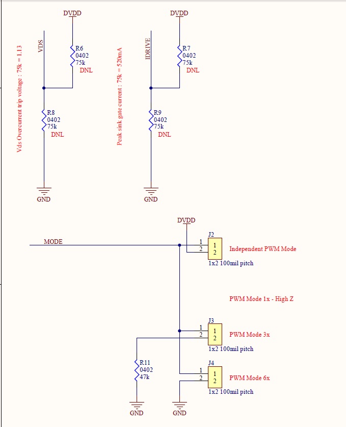
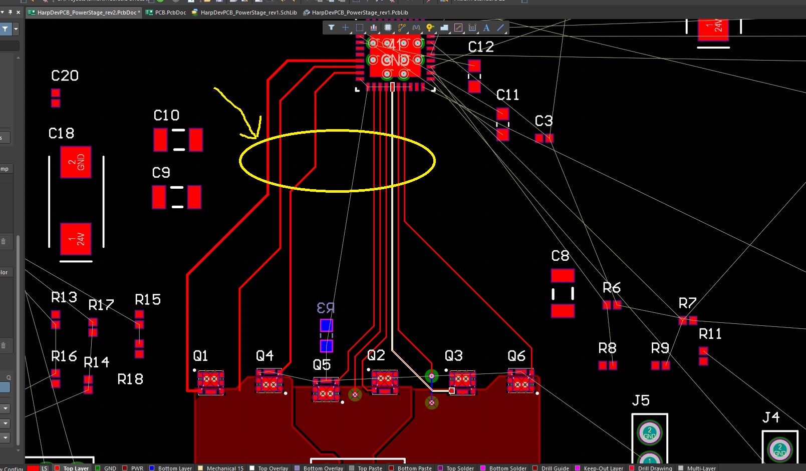
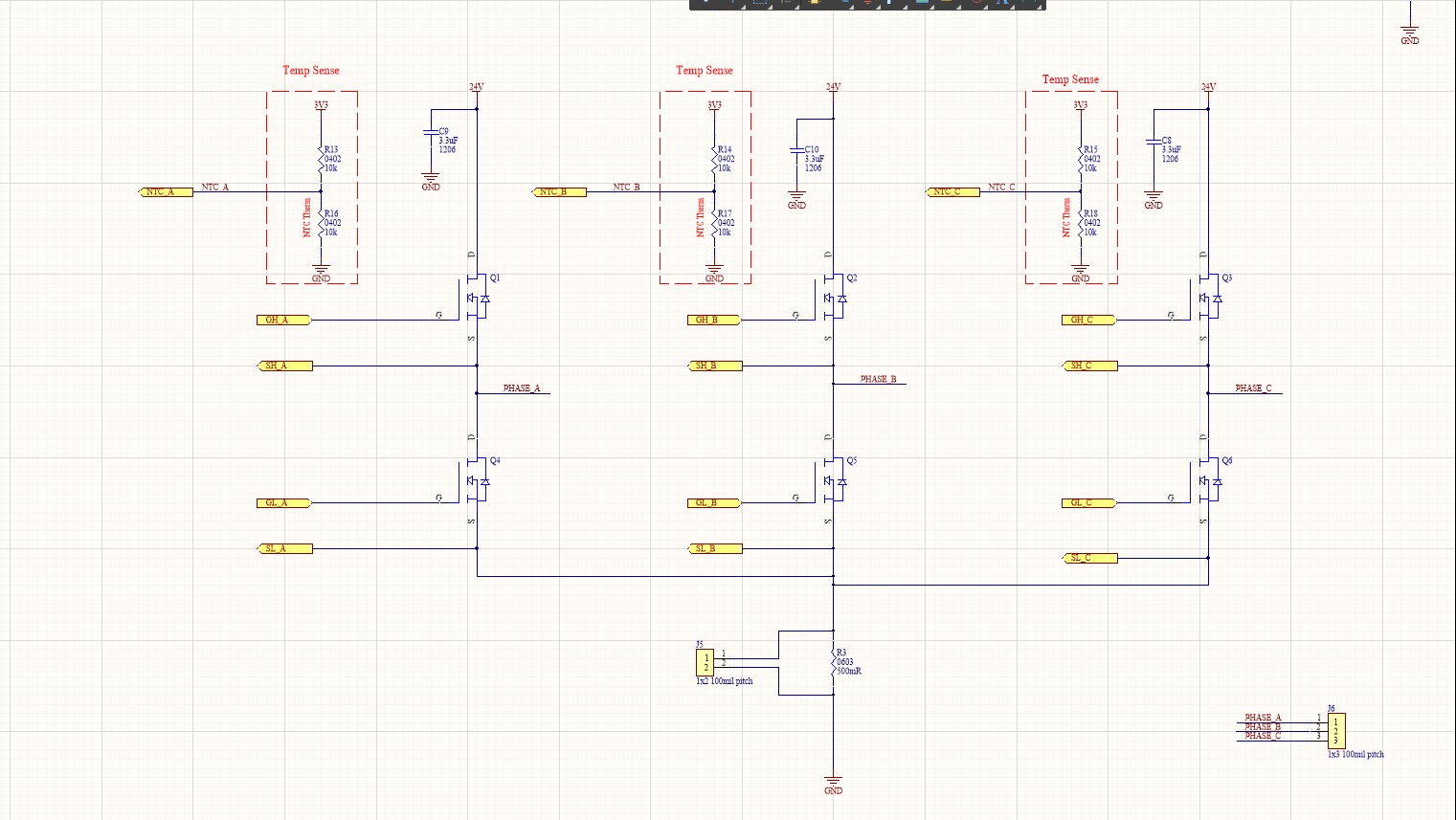
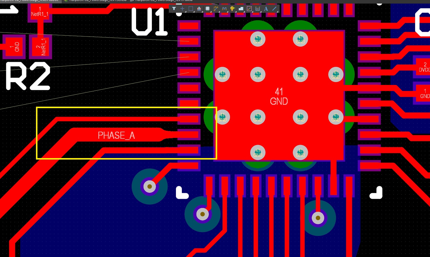
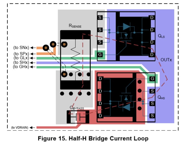
In reading through the datasheet for this part (hardware version with the buck regulator) I don't see any recommendations on the overall grounding scheme between AGND, PGND, GND and PAD.  All I've gathered is that AGND is for the DVDD linear in case you need a quiet low current supply?

1. Could someone clarify how I should connect up the AGND, PGND and GND relative to one another?  

1a. should all the ground be connected together if I don't need the DVDD output?

2. Is it correct to connect the thermal pad to the "gnd" net?

  • Robbie,

    All device grounds should be connected together, they should all be a low impedance connection to the system GND including power supply negative.

    The DVDD is used internally and is required for device operation. Even if you are not using this externally, it is required internally so datasheet guidance must be followed.

    Yes the thermal pad must be grounded.

    In general, all this guidance is available in the pin table, datasheet page 6.

    Regards,

    -Adam
  • Ok so my understanding is that all ground pins on the part should be connected to my single ground plane.  Is this correct?  I've attached screenshots of my schematic just for clarity.  The schematic represents my understanding.  

  • Robbie,

    Yes, your circuit now matches the DRV8323RH EVM schematic grounding. Can you show us the FET schematics?

    Regards,

    -Adam
  • Thank you Adam!

    Yes here are the FET schematics.  Some quick comments.

    I'm trying to use a resistor divider with NTC thermistors placed close to the fets to make sure they don't overheat.  Should my NTC thermistor dividers be connected to the Sources of Q4 Q5 and A6 or should they be connected to ground as shown?  I ask because I don't know it matters.  In layout the NTC thermistors won't actually be right at the FET source.  Not sure if this makes sense, but basically instead of connecting R16 to "gnd" for example, should it be connected to the source of Q4?

    Also, regarding the TI drive (DRV8320), are 8mil traces fine for signals GHA,SHA,GLA,SLA - GHB,SHB,GLB,SLB, GHC,SHC,GLC,SLC?  I have another screenshot of layout that shows them running from the driver to the FETs and they are 8 mil traces.  I am assuming these aren't high current signals.  Screenshot also below.

    Thank you so much for the support!

  • Robbie,

    Unfortunately I cannot comment on the thermistors, If it were me, I would ground them close to what was being measured as long as they don't interfere with the normal circuit operation.

    As for layout and trace widths, please review our layout guide:

    General Routing Techniques mentions 20 mil traces if possible. This is for current handling and signal integrity.

    Regards,

    -Adam
  • So is this what the guidelines in SLVA951  mean when they say the traces for GLx signal tracks should be 20mil min.?  This of course is wider than the pad on the actual DRV8320 part.

  • Robbie,

    Sorry, the guide that I linked got removed somehow, here it is again: www.ti.com/.../slva959a.pdf

    See section 4, it discusses trace width as well as transition from trace to via to pad.

    Regards,

    -Adam
  • Adam,

    Thank you for the updated link - that is a lot of good information!

    I have a question about SLVA951.  This app note also discusses layout guidelines for half H-bridge applications which is what I'm working on.  

    1.  Figure 15 shows the half bridge current loop.  I'm a little confused though because both FETs should never be on at the same time or you will experience shoot-through.  Why does this app note discuss the current loop as if the high side and low side are on at the same time?  In this application you have 3x half H bridges and current flows through one FET in two of the three H bridges at all times so that isn't what the actual current loop would look like right?  I'm a little confused.  I've attached a screenshot of figure 15 from SLVA951 that depicts this.

    2.  I have a single current sense resistor because I really only care about the average current through the overall motor - not each phase.  Is this a problem with efficiency and current loops?  I see in a lot of the layout recommendations and guidelines the current sense resistor is tightly coupled into the H bridge layout.  What are the ramifications of having a single current sense resistor and is this bad enough to warrant putting in substantial effort to have 3x sperate ones increasing the efficiency of the H bridge / FET power stage?

    Pics below

  • Robbie,

    You are correct, current doesn't flow through that whole loop that is shown, but that overall loop area is important. You're right that if current were to flow through that loop then we would have shoot-through. During one phase, the HS half of that loop flows and then during another cycle, the LS half of the loop flows. The document should explain that the intention is to keep that loop area from one HS to the other phase LS short and vice versa.

    One sense resistor is fine if that's all the information you need.

    Regards,

    -Adam