This thread has been locked.

If you have a related question, please click the "Ask a related question" button in the top right corner. The newly created question will be automatically linked to this question.

DRV8704: DRV8704EVM

Part Number: DRV8704
Other Parts Discussed in Thread: DRV8711EVM

Hello,

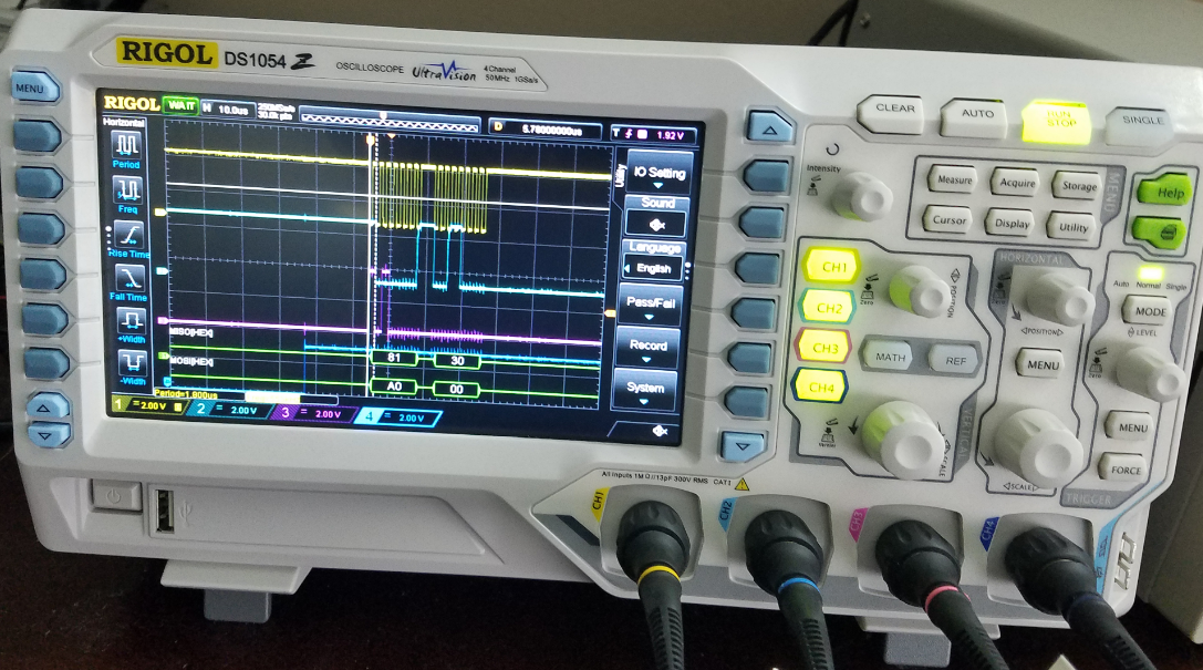
There is conflicting message on datasheet of the DRV8704 about the SCS PIN which I have highlighted on the attached picture.

When sending a SPI command/ message does the SCS PIN need to be HIGH or LOW?

From the diagram it seems to be high but the text says:

"To complete the read or write transaction, SCS must be set to a logic 0."

Is there any example code that shows SPI read operations for DRV8704 for Code Composer ?

Thanks,

Mikias Mekonnen

  • Hi Mikias,

    SCS must be high when sending a command to the DRV8704. To complete the command, SCS should transition from high to low.

    Please see the thread: https://e2e.ti.com/support/motor-drivers/f/38/t/620828 for an example scope capture.

    Also the firmware for the DRV8711EVM can be used as a code example. The operation of the SPI is very similar to the DRV8704.

    The firmware can be found here:  

  • Hello RicK,

    When I send 0b10100000(read bit and  OFF Register (Address = 0x02h)  and 0b00000000, I keep receiving 0x30 and I get any more data after that.

    Do you have any suggestions?

    Thanks,

    Mikias

  • Hi Mikias,

    Can you provide a scope capture of the transaction? If you have a two channel scope, please provide three scope captures

    1) SCS and SCLK

    2) SDATI and SCLK

    3) SDATO and SCLK

    0x30 is the correct response for the D7 through D0. D11 through D8 should have been 0bxxx1.

  • Hello Rick,

    I can see the data on the scope but I am not sure why I am getting 0X81 for the first byte plus I am only getting 0x30 in my buffer.

    Thanks,

    Mikias Mekonnn

  • Hi Mikias,

    Only bits 8 through 0 are relevant when reading register address 0x2. So 0x81 followed by 0x30 on the scope is correct for bits 8 through 0.

    If you are only seeing 0x30 in your buffer, are you reading your buffer at the end of each 8bit transmission?

    This appears to be a code issue, where the first 8bits (0x81) are overwritten by the second 8 bits (0x30).


  • Rick,

    Thanks, I have the reading part to work my clock was too fast.

    When writing to a register do I need to pay attention to the reserved bits?

    For example reg CTRL ==> 0x0, has bits 7-1 reserved and I want to update bit 0 which is part of the byte.

    Do you have an example of reg value that I can send the DRV8704?

    I tried sending the write bit, the register bits and  the value of the register which should look like:

    First byte 0x00000011 ==> write bit, the register bits, D8 and D9, 

    Second Byte 0x00000000 ==> make the ENBL bit 0.

    Thanks again,

    Mikias Mekonnen

  • Hi Mikias,

    The best approach when dealing with the reserved bits is to read them, and use the default values when writing to the registers.

    Writing a 1'b0 in each reserved location will also work.

    For example reg CTRL ==> 0x0, has bits 7-1 reserved and I want to update bit 0 which is part of the byte.

    I tried sending the write bit, the register bits and  the value of the register which should look like:

    First byte 0x00000011 ==> write bit, the register bits, D8 and D9, 

    Second Byte 0x00000000 ==> make the ENBL bit 0.


    This is correct if you also want to set the dead time to 410ns, gain to 40, and disable the motor.

    Writing to disable the motor is a good test. This is easily confirmed by setting the xIN1/2 inputs to 1 and 0 respectively and measuring the outputs before and after writing to disable the motor.