This thread has been locked.

If you have a related question, please click the "Ask a related question" button in the top right corner. The newly created question will be automatically linked to this question.

DRV8842: Input Requirement

Part Number: DRV8842
Other Parts Discussed in Thread: DRV8840

Hello,

I would like you to confirm whether following input is allowable or not.

* Input "HIGH" level(100% duty) to both IN1 and IN2 for DRV8842.

 According to datasheet of DRV8842, min "Externally applied PWM frequency" is defined as "0 kHz". It seems that user can input 100% duty signal to IN1 and IN2.

On the other hand, I found DRV8840. Input interface of this device is defined "PH/EN". (I'm not sure what is different between DRV8842. Because DRV8842 also allow 100 duty cycle.)

I confirmed logic table of H-Bridge.

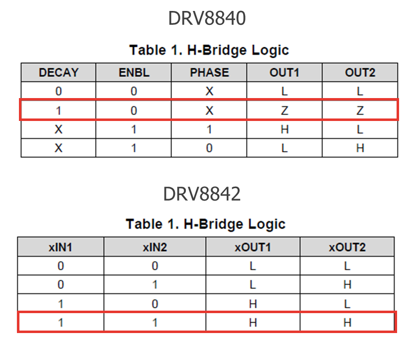
According to above, DRV8842 have both output High state. (In this case, If user use 100 duty cycle as PWM, I think there is no chance to reduce current.)

So, the question is below.

* Does DRV8842 actually allow 100% duty for high level to IN1 and IN2 pins ?

Thanks in advance,

  • Hi Machida-san,

    Yes, the DRV8842 does allow 100% duty for high level to IN1 and IN2 pins.

    Current will decay slowly if this is setting is used.

  • Hello Rick-san,

    Thank you for your reply.

    Understood.

    My customer is facing issue which they sometimes observe that motor suddenly stop after rotating for few minutes. So, at first, I suspected that this device does not accept 100 duty signal to INx because I'm not sure difference b/w DRV8842 and DRV8840.

    To solve this issue, please continue to discuss on this thread.

    Customer also confirmed that nFault is asserted when motor stop. According to datasheet, nFault will assert in case of OCP or TSD.

    They confirmed Motor current by using current probe (and also checked ISEN voltage). And confirmed package temperature.

    However, they said that both were no problem. The questions are

    1. Is there any event which nFault is asserted except OCP or TSD ?

    2. If current is over chopping current which is set by ISEN and VREF, is nFault also asserted (It seems that OCP is defined as 6A from datasheet, so I ask) ?

    Best Regards,


  • Hi Machida-san,

    If the fault is OCP, the outputs will remain disable until either nRESET is toggled, or power is removed and re-applied. Toggling nSLEEP will also reset the OCP.

    If the fault is TSD, the outputs will re-enable after the device temperature lowers to a safe level.

    Assuming that the fault is OCP, please check the following:

    1) How many boards exhibit this behavior? How many do not?

    2) Does the customer have a 0.1uF capacitor across the ISENSE resistor? If not, please add one and re-try the experiment.

    3) Is it possible one of the two device output pins is disconnecting from the PCB? This could create a condition where all the current flows through one FET instead of two.


  • Hello Rick-san,

    1) How many boards exhibit this behavior? How many do not?

    => They said two. (I'm not sure exact parameter.)

    2) Does the customer have a 0.1uF capacitor across the ISENSE resistor? If not, please add one and re-try the experiment.

    => Yes, Implemented 0.1uF on ISENSE.

    3) Is it possible one of the two device output pins is disconnecting from the PCB? This could create a condition where all the current flows through one FET instead of two.

    => Do you mean about below ?

    * Disconnect one of pin5 or pin10 for OUT1. And disconnect one of pin 7 or pin 8 for OUT2.

    I would like to share more detail, so could you please tell me your email address ?

    Best Regards,

  • Hi Machida-san,

    What type of fault was identified by the customer, overcurrent or overtemperature?

    3) Is it possible one of the two device output pins is disconnecting from the PCB? This could create a condition where all the current flows through one FET instead of two.

    => Do you mean about below ?

    * Disconnect one of pin5 or pin10 for OUT1. And disconnect one of pin 7 or pin 8 for OUT2.

    I would like to share more detail, so could you please tell me your email address ?


    If one of the output pins or sense pins disconnect from the PCB (pin 5/10, 7/8, 6/9), the current flow path is changed. If this happens, an overcurrent event could occur.

    This could happen if the PCB is hand soldered.

    I will make arrangements for you to share more detail.

    If possible, please capture the current through the load just prior to nFAULT going low. The scope should be zoomed in to ~5us/div.  


  • Hi Rick-san,

    Let me confirm one thing.

    What value OCP time is defined ?

    It seems there is no info in datasheet.

    Best Regards,

  • Hello Rick-san,

    I sent private message today.

    Can you get it ?

    BR

  • Hi Machida-san,

    Yes, I did receive the message.

    I will reply by Monday.

    For now, the thread will be marked as resolved.  Any generic findings that help the community may be reported here.