This thread has been locked.

If you have a related question, please click the "Ask a related question" button in the top right corner. The newly created question will be automatically linked to this question.

DRV8303: Reverse Polarity Protection FET Gate Drive

Part Number: DRV8303

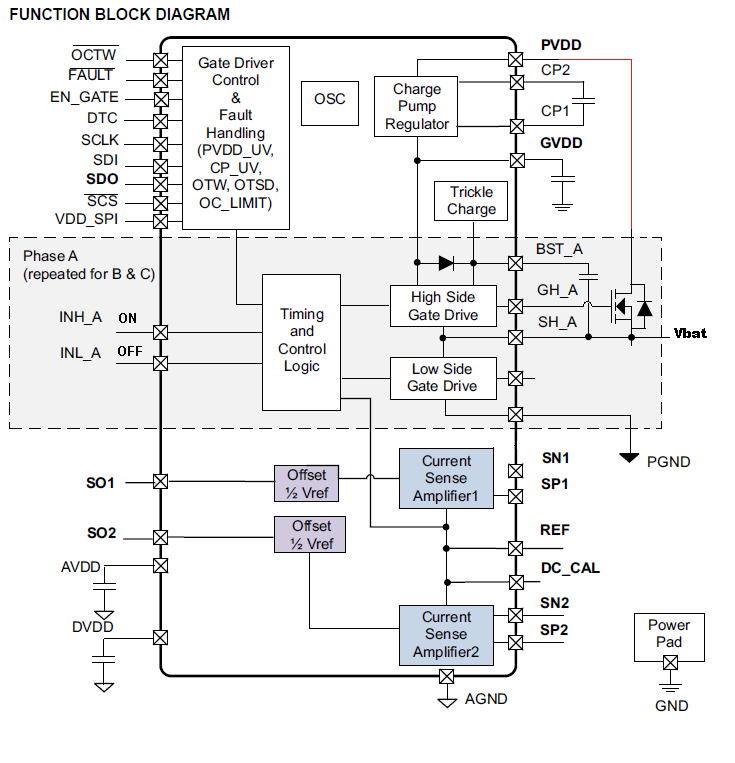
A while ago I asked if the DRV8303 could supply gate drive for a reverse polarity protection connected FET. When power of the correct polarity is applied, the substrate diode of the FET power up the circuit. The driver chip then turns on the FET and shorts out the substrate diode to reduce the power lost. The circuit works as planned when correct polarity is applied but fails under reverse polarity. The trace from Vbat to SH_A burns up and the chip smokes.It seems the SH_A pin to ground cannot handle reverse voltage. I replaced the driver chip and left the connection from SH_A to the BST  cap open and the gate drive still works and the circuit can handle reverse voltage without a problem. When i connected the BST cap to the SH_A  pin  but left the connection to Vbat  open the gate voltage would only rise to 1.4 v.olts with greater that 6 volts applied on Vbat. When the BST cap was removed from the circuit the gate voltage could then rise to a level that turned on the FET (Vgs = ~11 V). Any thoughts on this implementation of the chip? Also why is the gate voltage limited to 1.4 volts ( 2 diode drops?) ?

 `

  • Michael,

    Let me check on this and get back to you later today.

    Regards,

    -Adam

  • Michael,

    I am not fully understanding the different cases you mention above with the VBAT/BST/SHA variations, could you show schematics for the various cases and the resulting operation?

    Regards,

    -Adam

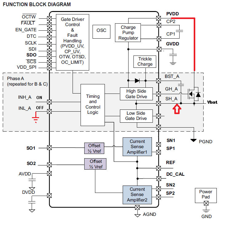
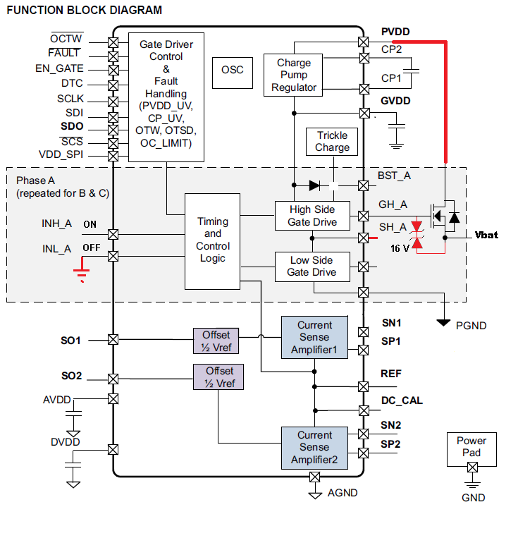
  • I first tried the circuit shown below. The circuit worked with the correct polarity. The FET substrate diode powered the chip and then the trickle charge circuit applied gate voltage to the FET and turned the channel on. Reverse polarity smoked the driver chip and burned the trace going to the SH_A pin.

    It seems the SH_A pin can not handle reverse polarity to ground.

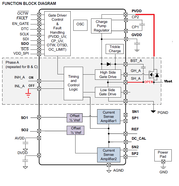
    I replaced the chip and left the SH_A connection open. this connection worked as hoped. With the correct polarity the FET turned on and with reverse polarity nothing happened.

    As third experiment I connected the boot strap capacitor to the SH_A pin but did not connect the SH_A pin to Vbat. This time the voltage on the gate seemed to be clamped at 1.4 volts. Since the source of the FET was at Vbat the FET never turned on.

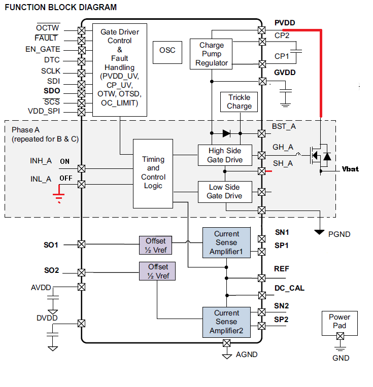
    The last experiment was to leave the bootstrap capacitor off completely. The circuit worked as hoped.


    Do you see any problems using the chip in this last configuration?

    I was thinking of putting back to back connected 16 volt zener diodes across the gate to source of the FET.

    Also could you explain why having the bootstrap capacitor connected to the SH_A pin would prevent the turn on of the FET.

  • Michael,

    I realize that you are not in fact using the low side and high side FETs in your circuit. You also are not driving a motor, is this correct?

    Regards,

    -Adam

  • Adam

    You are correct.

    The driver chip is configured for 6 wire communication with the micro. All of the half bridge drivers have the low side input grounded.

    One of the drivers is used to drive the reverse polarity FET.

    The other 2 sections are controlling high side FET's driving solenoid loads with freewheeling diodes.

    The entire system has 6 other DRV8303 driving 18 other output circuits. Some high side and some half bridge connected outputs. 

  • Michael,

    My apologies for not realizing this sooner. It is rare that our drivers are used like this and I assumed you were trying to drive a normal half-bridge or motor.

    The BST isn't needed if you don't plan on using a half-bride where the source of the high side FET is intended to stay at VBAT while the High side FET stays on.

    The reason why the DRV was likely dying while the BST was installed is because if your SH node was not at zero when the charge pump attempts to charge the BST cap, the BST voltage is reduced by the voltage sitting at SHx. Then when the FET attempts to turn on, the charge pump has to work much harder to keep the FET on because of the reduced BST voltage, overworking it. 

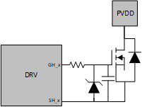
    One recommendation I do have for when not using the BST cap is to install a Cgs cap and series gate resistor which will help ensure if your VBAT fluctuates that the charge pump and associated circuit doesn't have to struggle to regulate the gate voltage.

    I don't have a great suggestion for the value of cap but something less than 100 ohms should work. 

    Regards,

    -Adam

  • One additional question. I was a little worried about the voltage on the gate of the FET during loss of Vbat during normal operation. I was thinking of putting two back to back series connect 16 volt zener diodes across the gate and source of the FET to limit the voltage. Do you see any problems with this?

    mike

  • Mike,

    Could you show us a schematic/image of this configuration to be sure?

    Regards,

    -Adam

  • Added Zener diodes for gate voltage protection.

  • Michael,

    This clamp will help protect against Vgs overshoot (we actually have this built into most of the DRV devices internally but yours will be disconnected) but back to back diodes aren't really needed.

    In the end I would recommend reconnecting the source connection with the series gate resistor and Cgs cap so that the FET has a good discharge path.

    Without the Cgs cap the charge pump has the sole responsibility of charging the boot strap if the VDRAIN spikes. 

    Regards,

    -Adam

  • Could you provide a schematic to show exactly how the resistor and capacitor are to be connected?

    mike

  • Mike,

    Hopefully this helps:

    Regards,

    -Adam

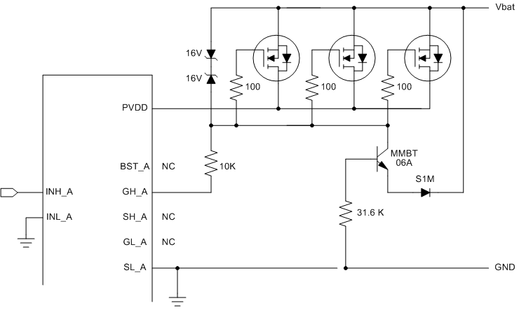
  • Here is the proposed circuit. Where would the resistor and capacitor go?

  • Adam

    In your circuit PVDD goes to the 8303. Battery power comes in through the source of the FET. If the source of the FET is connected to SH_X and reverse battery power is applied the chip smokes. The ground to SH_X connection can not handle reverse polarity. 

    mike 

  • Michael, 

    Thanks for the explaination. 

    Looking at your latest schematic, this should work fine. The only thing I would add, optionally, is a Cgs capacitor between the gate and source of each FET. Make sure this is on the FET side of the gate resistor.

    Regards,

    -Adam