This thread has been locked.

If you have a related question, please click the "Ask a related question" button in the top right corner. The newly created question will be automatically linked to this question.

UCC27531: Just Blown up a UCC27531 driver and don't know why, or how to fix the design

Part Number: UCC27531
Other Parts Discussed in Thread: MSP430F2013, MSP-FET

I've just blown up a UC27531 and I am at a loss as to the reason why. It's the first time I have used this driver so I have no experience with it at all.

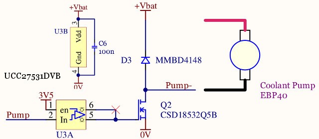
The circuit :-

The "Pump" PWM signal is driven from an MSP430F2013 port, at 25 kHz with a duty cycle of 14 to 100 %

+Vbat is a 12V battery, and the pump draws 5A pk. The motor is brushless with an internal controller of unknown design. It has been tested successfully on a commercial PWM driver.

I have been testing the program/cicuit with a resistive load, but it failed withing seconds of turning it on. The MOSFET is fine, but the driver output is shorted to ground, I am at a loss as to the exact mechanism that killed the 2.5/5A device, but I assume it has something to do with the gate - drain Miller capacitance of Q2 and my lack of gate current limitation. I am surprised that the gate current could reach beyond 2.5A though, but admit that i did not do any calculations, in part because I don't know how.

I went to some trouble to follow the layout suggestions. In particular, the source and return traces (U3 - Q2) are parallel and their lengths are minimised. Similarly for the onboard traces to the pump.

Can someone explain the failure and suggest the design procedure that I should have used to prevent it?

  • NB: it failed when connected to the pump, not on the resistive load.
  • Hi Errol,

    Sorry to hear of your trouble.

    I only see 100 nF of decoupling on your Vbat, do you have additional decoupling on this supply?
  • Hello Don, thanks for your help.
    I've got 100 nF at Vdd (+Vbat) on that driver. There is another driver that I'm not using at present, with 100nF across it as well. Nothing more though.
  • Hi Errol,

    Thanks for reaching out to us, my name is Mamadou Diallo, I will help address your concerns.

    It seems like there is a reverse current at the driver output from Cgd(occurring due the oscillation from interaction between Cgd and the source inductance of the MOSFET) which could cause damage to the driver.
    Consider adding a series gate resistor on pin 6 (OUTH ONLY!) of the driver and leaving pin 5 as it is which would limit the MOSFET's turn-on speed and maintain the turn-off speed. It would also help take some power dissipation away from the driver as without a gate resistor , the total gate drive power being dissipated entirely in the driver.

    Additionally, consider adding a second decoupling capacitor (1uF) in parallel with C6(100nF) to prevent the driver from pulling VBat under the UVLO threshold and mitigate any effects of ground bounce on the driver.
    Voltage spikes on the main power rail during switching could also damage the driver if you don't have any/enough decoupling capacitance in your circuit.

    Once we make these changes, you can test on the resistive load (which was already working as you previously described) before adding the pump.

    Also consider these app notes for common gate driver fundamentals topics that you may find helpful for current and future projects.

    www.tij.co.jp/.../slla387.pdf (Understanding peak source/sink currents)
    www.ti.com/.../slua618.pdf (Gate driver fundamentals)
    www.tij.co.jp/.../slla385.pdf (Understanding Peak Source and Sink Current Parameters)

    Let's make those changes first then if we're still having issues, we'll further debug. If no issues at that point, please press the green button to confirm that we helped resolve your issue.

    Thanks.

    Regards,

    -Mamadou
  • Hello Mamadou,

    how would one calculate the value of a series gate resistor?

    I have since read all of the app notes you mentioned, none of which make any suggestion of how to calculate a series gate resistor

    I noted that the data sheet mentioned as a note that parameters were measured with 1uF decoupling, so I have just now added one.

    regards, Errol

  • Hi Errol,

    On the turn on path for example, the series gate resistor will create an RLC resonant circuit with the internal input capacitance and the source inductance of the MOSFET and other parasitics (pcb traces). The primary role of this resistor is to help reduce power dissipation in the  driver, limit ringing caused by parasitics and capacitances mentioned, also limit the ringing caused by dv/dt and di/dt and fine tune gate drive strength to optimize switching losses. Section 2.8 of the Gate driver fundamentals app note I previously attached discusses this and also the external gate resistor selection guide below gives an approach of determining this parameter using the Q-factor:

    www.tij.co.jp/.../slla385.pdf

    However, you can also estimate it by determining how much delay you want your design to tolerate and then using tao = time constant =  Rgate * Ciss (MOSFET datasheet) and then fine tuning the resistor to your desired goal. I have seen gate resistor anywhere from 2 ohm to 10 ohm.

    Please let me know if your design is still having issues or if you have other related questions and I will happily help address them. 

    Thanks.

    Regards,

    -Mamadou

  • Hello Mamadou,

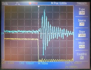
    Not knowing how much delay my design will tolerate, I took a stab and made the gate resistor Roh = 5 Ω and Rol = 0 Ω. The driver was much happier about that, since it survives - on a resistive load with 2.5 A peak current. The switch off needs addressing though, since it causes havoc on the uC supply

    The blue trace is ac coupled to the Vdd/Vss pins. That's 300 mV pk, which for some reason is fine with a low PWM duty cycle, but as it is increased, at some point the micro (MSP430F2013) stops/gets lost, including the Timer-A derived PWM, So it is more than just getting lost in it's program. It does recover by cycling the power though, but I think this IC will not be used for anything more than development. The supply is 3.5V, so the noise takes it to 3.8V, just below it's absolute maximum of 4.1V

    I don't know why increasing duty cycle would be at issue, as the frequency doesn't change. Perhaps the ringing extends into the switch-ON pulse and that is creating even more noise, causing the uC to stop. I haven't seen what happens at this point in time though,

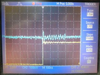
    Switch ON is fine at under 100 mV pk and virtually no ringing. Over-damped I suppose.

    So I need to add some resistance in the OUTL line. Some more aggressive uC supply filtering wouldn't go astray either. I can't do a lot about the ground plane currents at present, but that needs some more thought with a new layout.

    I assume that the Roh / Rol ( Rg ) limit will be that which heats up the MOSFET intolerably, due to the increased switching time, ie. time spent in the linear region.

    So it is coming together. Thank you for your help

  • Hi Errol,

    I'm glad to hear the driver happy with the suggestion.
    The issue on blue waveform may be related to the bypass capacitor from the uC. The quiescent current can vary by as much as 10x factor depending on the input state which is leading to the duty cycle dependency of ripple accross VDD-VSS.
    This cap should be the same value as that of the driver and you can estimate using:
    C = [Iq,hi * (Dmax / fsw) + Qg] / Delta V
    where Iq,hi is the quiescent current of the driver when its input high
    Dmax = max duty cycle that the driver can stay high
    fsw = switching frequency
    Qg = total gate charge
    delta V = voltage ripple

    If you solve for the ripple voltage, you can see how the ringing you're observing is dependent on the duty cycle. Consider adding a 1uF decoupling capacitor to the uC supply.

    Also you're right, we should add a second resistor Rol (e.g) 2 ohm which would solve turn off issue along with the above recommendations. Increasing gate resistance slows down turn on/off speed of the MOSFET which leads to it spending more time in linear region but those resistor help with the driver power dissipation. It's a trade off.

    Also consider sharing your next design/schematics/layout and we will happily help review it.

    Please let us know if you need further assistance or press the green button if this helps resolve your issue.

    Thanks.

    -Mamadou
  • Hello Mamadou,

    I have set Roh=Rol=Rg=5 Ohms, and the noise has almost disappeared. The uC supply now has filtering both pre and post, and Vdd noise is now normally < 100 mV p-p. So, on the surface, the circuit is now well behaved.

    EXCEPT for a very strange spurious mode it gets into at one particular duty cycle setting, close to 100%, when the uC P1.2, the PWM output, which should go no higher than 3.4V (Vdd),   suddenly pops up to just over 5V.   The noise on the uC Vdd is very low now, during normal operation   but increases significantly during this spurious activity 

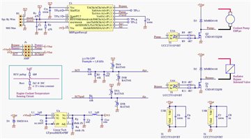
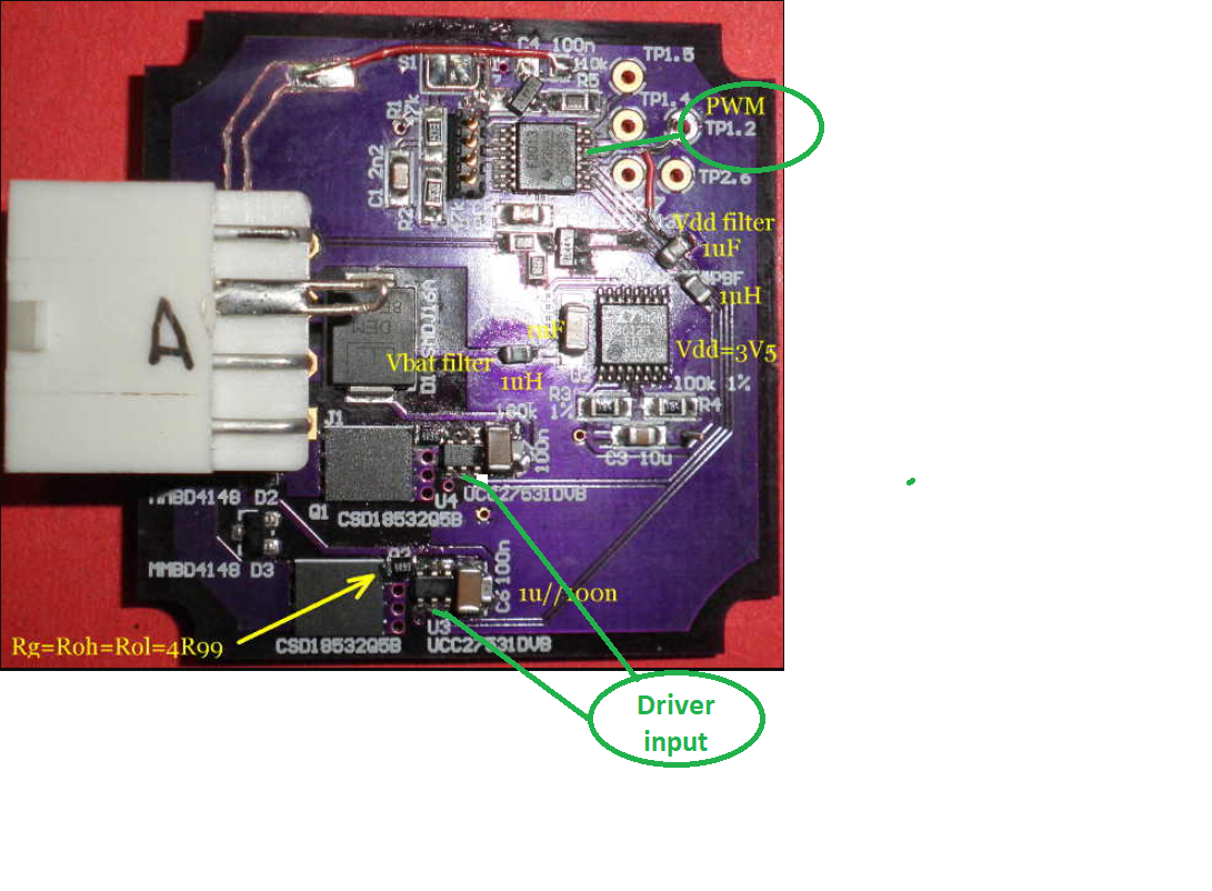
    The revised circuit :-   The Rg resistors are not separated in my much modified board, but everything else is as per the circuit. The mods :-  The gate drive traces are well confined, minimising inductance and emissions. The traces to / from the Mosfet are also closely coupled and separated from the uC ground plane.

    The 'en' inputs to the driver have been disconnected from the 3V5 supply, and depend purely on their internal pullups to their Vref supplies. Measuring Ven, this Vref appears to be ~ 5V, and since this is the only 5V source on the board, it appears to be the source of the spurious operation to 5V of the PWM port.

    So, I'm still struggling.

    (Not only with this, but it appears that my MSP-FET430UIF debugger has also not enjoyed the experience, and will no longer communicate with the uC. I have three boards, and none now talk to the debugger, although all still run as per the above. I have a new MSP-FET on order.)

    I appreciate your continued help,

  • Hi Errol,

    Sorry to hear that the design is still giving you hard time.

    Couple of comments/suggestions:

    1. I didn't really catch the gate resistors current setup:

    "The Rg resistors are not separated in my much modified board" Do you mean by this statement that Roh and Rol are not split and are just one single resistor? Correct me if I am wrong but I only see one resistor on your layout. You should use 2 separate resistor if you're not: one for the source current path and the second for the sink current path.

    2. Very interesting behavior from the p1.2 port. If the enable pin of the driver at 5V is the cause of the spurious event you described during high duty cycle event, does P1.2 still follow EN pin voltage of the driver when the EN pin is connected to 3V5 supply? To test it out, maybe tying EN pin to VDD or different supply could tell but if it is the case, but P1.2 pin voltage might exceeds abs max ratings and cause damage.

    3. From the layout, you did a good job on the power stage/output with the short traces and closed-knit connections but I noticed the PWM signal on the top right and the driver input (bottom) quite distant from each other. You want to avoid long traces also at the input because ground from power stage is the same as the input stage.Switching from the MOSFETs and high di/dt coupled with pcb board layout parasitics can cause GND bounces which can interfere with the differential voltage between IN pin and GND. Even though though we are filtering,these long input traces can mitigate effectiveness of the filters.

    4. "(Not only with this, but it appears that my MSP-FET430UIF debugger has also not enjoyed the experience, and will no longer communicate with the uC. I have three boards, and none now talk to the debugger, although all still run as per the above. I have a new MSP-FET on order.)"

    Unfortunately, I am afraid I am not going to be of much help with MSP-FET430, I can pull the expert team supporting that device so they can help us suggest answer once we've resolved our gate driver issue.

  • Hello Mamadou,
    1. Roh and Rol are not split on the modified board and are just one single resistor. I'll split them as you suggest (as shown in the schematic) and see what happens.

    2. the enable pin was originally connected to the uC Vdd (3.5V) but had been disconnected completely before the recently reported test. It now relies solely on it's own internal pull-up. The only connections between the PWM driver (U3) and the uC are P1.2 and ground. Teh enable pin can not therefore be the source of the spurious 5V event.
    The second Mosfet & driver (Q1, U4) you can see above the PWM power stage (Q2, U3) is purely to power a solenoid. It doesn't switch during any of the current tests. It is not connected to a load at present. It's input source is P1.0

    3. The driver input traces are longer than they could be. On the next design I'll swap the 3.5V supply and the uC positions. That will halve the trace lengths.
  • Hi Errol,

    1. Thanks for making the suggested corrections.

    2. Looking at the schematic again and I see the uC Vcc is C11=100nF which could explain the noise present there. Consider replacing it with C11 by 1uF instead if you haven't already.

    3. Good to hear. Keep in mind when using these drivers, you uC output to driver input traces to be as short as possible and more importantly, locate the driver as close as possible to the power device in order to minimize the length of high-current
    traces between the output pins and the gate of the power device(you did an excellent job on this!!). Also the turn-on and turn-off current loop paths (gate driver , power MOSFET and VDD bypass capacitor) must be minimized as much as possible in order to keep the stray inductance to a minimum.

    Please let me know what we get once the changes in 1. and 2. are made.

    Thanks.

    Regards,

    -Mamadou
  • Hello Mamadou,

    1. I've split Roh/Rol into two, as suggested, with no improvement

    2. C11, as shown on the circuit isn't actually installed. C10, a 10 uF cap is about 7 mm from the uC Vdd pin. This is not going to be as good at high frequencies as a smaller cap, so I will add one as per the circuit. However, I doubt if it will make a lot of difference to this problem, as the noise is quite acceptable outside of the spurious operation. We'll see.

    I think that the MSP430 is quite capable of being powered spuriously via a port, as it needs very little current to run. My next step is to remove the driver completely, and connect the PWM directly to the Mosfet gate. The switching won't be as fast, and the power dissipated in the Mosfet will be higher, but this will remove the driver from the mix, and confirm, or otherwise, it's contribution to the problem. But this will have to wait for a week or so, as I've been called away on another errand.

    I appreciate your help.

  • Hi Errol,

    Thanks for the updates and sorry that the circuit is still not up and running.

    That action plan seems like a good idea as well, whenever you implement those changes, please let us know via a new thread of here so that we can get to the bottom of this. If without the driver, you're still experiencing this issue, then we might need to pull the MSP430 team to further assist.

    In the meantime i am going to close this thread until I hear back from you.

    Thanks.

    Regards,

    -Mamadou
  • At this juncture, I need to take the next step, already defined, to get to the bottom of this. I'll open a new thread when I know more.