This thread has been locked.

If you have a related question, please click the "Ask a related question" button in the top right corner. The newly created question will be automatically linked to this question.

LM98620: Analog input range and datasheet

Other Parts Discussed in Thread: LM98620

Hi,

I would like to use the LM98620 6 Channel Imaging Signal Processor to interface with a 6 channel CIS from Rohm, one that is similar to the LSH1208-BD70A

However, I don't quite understand the actual analog DC input range of the component. The datasheet specifies a recommended common-mode voltage of 1.65V at each OSR input. In addition, the input range of the ADC seems to be set at 0.98V to 2.23V. The CIS I want to use outputs a voltage between 0.8V (= dark pixel) and 2V (= light pixel). If the input is biased at 1.65V during a dark pixel output voltage (as is suggested) and the CIS output is then increased to the value of a white pixel, the OSR input would become  2.85V, which is clearly above the top voltage reference of the ADC.

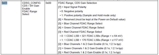
Therefore, the mentioned 'Maximum Input Level' of 1.2Vpp seems to be the valid bipolar voltage range, which is not suited for my application? The datasheet does mention an "Input Signal Polarity Select" option, but I don't understand what this option does or what it implies.

In addition to the above ambiguity, the datasheet provided on the component product page (LM98620) seems to be unclear or not complete on quite some points. Am I correct that this datasheet is a reduced version of the complete one, which is available under a NDA?

Thanks in advance!

Best regards,

Sander Lybeert

  • Hi Sander,

    Please allow till tomorrow afternoon for a response from me.

    Regards,

    Hooman

  • Hello Sander,

    I've tried to respond to your questions below in color.

    **************************************

    Question 1: However, I don't quite understand the actual analog DC input range of the component. The datasheet specifies a recommended common-mode voltage of 1.65V at each OSR input. In addition, the input range of the ADC seems to be set at 0.98V to 2.23V. The CIS I want to use outputs a voltage between 0.8V (= dark pixel) and 2V (= light pixel). If the input is biased at 1.65V during a dark pixel output voltage (as is suggested) and the CIS output is then increased to the value of a white pixel, the OSR input would become  2.85V, which is clearly above the top voltage reference of the ADC. Therefore, the mentioned 'Maximum Input Level' of 1.2Vpp seems to be the valid bipolar voltage range, which is not suited for my application?

    [Hashemi, Hooman]  4/8/14: The LM98620 input stage has a linear range from 1.05V to 2.25V. This is derived from knowing a 1.2Vpp linear range and its center being at 1.65V. As Figure 15 shows, the input is AC coupled and then clamped internally. This is the swing value you should be using and you won’t be over-driving anything assuming you have setup your clamp properly.

    In your case the sensor appears to have a 0.5V maximum swing (dark or reference to full white), as shown below, which if added to the 1.65V clamping voltage gives 2.15V. This fits within the common mode range (1.05V to 2.25V) with no problem.

    If your sensor signal were larger, you  can provide your own clean low impedance Vclp voltage and connect that to the Vclp ext pin instead of using the Vclp int as the source. But, you don't need to do that with your sensor.

    It is possible to DC couple into the LM98620 if the sensor has a reference voltage of around 1.05V (yours does not), eliminating the need to do AC coupling and clamping, to offset the sensor voltage within the AFE common mode range.


    Question 2: The datasheet does mention an "Input Signal Polarity Select" option, but I don't understand what this option does or what it implies.

    [Hashemi, Hooman]  4/8/14:  From your sensor’s (LSH1208-BD70A) datasheet page 3, diagram (a), it looks like your sensor output is positive going. So, in register 0x03h, you would set bit 7 to 1 for positive polarity.

    Question 3: In addition to the above ambiguity, the datasheet provided on the component product page (LM98620) seems to be unclear or not complete on quite some points. Am I correct that this datasheet is a reduced version of the complete one, which is available under a NDA?

    [Hashemi, Hooman]  4/8/14:  What you currently find for LM98620 on the web is the entire / complete datasheet. At one point, an NDA was required but not anymore.


    ************************

    Regards,

    Hooman

  • Hello Hooman,

    Thank you for your extensive answer!

    I understand your explanations, but it is still unclear to me what the "Input Signal Polarity Select" option does. If I were to use the Vclp internal as the source for the input clamping and the corresponding input range from 1.65V to 2.25V, I would only use half of the complete input range of 1.05V to 2.25V. Doesn't this mean that I lose half of the valid input range of the ADC, thus one bit of conversion accuracy? Or is the actual valid input range of the ADC affected by the "Input Signal Polarity Select" option?

    If this is the case, what happens when I use a self-chosen Vclp of (for example) 1.05V to obtain an input dynamic range of 1.2V?

    I ask this because I have done some measurements on the sensor I mentioned, and these have shown that the outputs of the sensor can easily achieve voltages of more than 2V. I am still unsure about the dynamic range I will be using in my application, so it would be nice if I have some degree of flexibility at the input of the AFE.

    Thanks in advance!

    Best regards,

    Sander

  • Hello Sander,

    1. Polarity Setting: Positive polarity means more white results in more positive sensor voltage. Neg. polarity is a lower voltage with more white pixel. Most CCD sensors are negative polarity. Many CMOS and CIS are positive (with exceptions). Polarity select gives you that flexibility so that AFE digital output will always give higher digital value for more white, if polarity bit is set properly.

    2. Input Voltage Range: The voltage range I've been quoting is for the benefit / linearity of the front end. There is additional analog offset and analog gain (having a very wide range and reach) which are incorporated inside the LM98620, as shown on page 3 Block Diagram. Even if your input swing covers only half of the front end linear range, this does not mean your digitized output is missing 1/2 the dynamic range / bit count. If you have a choice, it is always best to go with as big an input as possible, and then use less gain within the AFE for higher performance.

    For your particular large input condition, you can break the external / board connection between VCLPINT and VCLPEXT (and still use a large cap on it), as shown in Figure 15. Assuming a negative going signal, you would then use VCLPEXT voltage close to the top end of the input voltage range 2.25V as the best setting for your input.

    Regards,

    Hooman

  • Hello Hooman,

    We also have some problems implementing the power supply for this device. There is a relation defined for the different power supplies. VDDD should be greater then VDDA and VDDD should be greater then VDDLVDS. And then some schematic is drawn in figure 3 how to do this. But that is all that I find in the datasheet.

    Are there tolerances on this rule?
    Is it only for power sequencing (can we use different regulators for this)?
    What are the values of the components in figure 3 ?
    What is the maximum ripple allowed on this device? (if I follow the operation conditions then the chip will work with a ripple of 0.6V, I don't find the PSRR either)

    Kind regards,
    Koen

  • Hello Hooman,

    just jumping on this thread as per similar questions I've got from Sander through a different loop.

    Sander : here below copying in red some of your questions so far. Btw questions on analog DC input range and Input Signal Polarity Select were already answered by Hooman.

    - Does there exist an eval board we can share with the customer?

    Here Hooman recently answered to a similar point as follows : "..The LM98620 EVM is not posted to the web and it is not currently offered to customers.." ->> Hooman please confirm this statement still holds or not

    - Do you have a usermanual discribing more in detail the operation mode?

    Hooman, I'll let you answer on that :-)

    Thanks in advance to all to close the loop here all together, best regards

    Sergio

  • Hello Sander, Sergio, and Koen,

    My responses in color by <HH 4/22/14>: 

    1) We also have some problems implementing the power supply for this device. There is a relation defined for the different power supplies. VDDD should be greater then VDDA and VDDD should be greater then VDDLVDS. And then some schematic is drawn in figure 3 how to do this. But that is all that I find in the datasheet.

    <HH 4/22/14>: The datasheet calls this out on page 8:

    VDDD ≥ VDDA,

    VDDD ≥ VDDLVDS

    So, VDDD can be equal or greater than VDDA (not just greater than). The easiest way to implement this is by using a single LDO for all 3 power supplies (as Figure 3 shows).

    2) Are there tolerances on this rule?
    Is it only for power sequencing (can we use different regulators for this)? 
    What are the values of the components in figure 3 ?
    What is the maximum ripple allowed on this device? (if I follow the operation conditions then the chip will work with a ripple of 0.6V, I don't find the PSRR either)

    <HH 4/22/14>: You can use separate regulators but there is no advantage to this and you must comply with the relationships shown above ( ≥ ).


    It is understood that high speed, high resolution ADC devices would not have Precision type PSRR ratings. It is expected that the LDO / linear-regulator used to generate the supplies would have low ripple ( < 25mVpp).


    3) Do you have a user-manual describing more in detail the operation mode?

    <HH 4/22/14>:  Unfortunately No.

    If you post your questions here, I'll try to respond thoroughly and quickly.


    Regards,

    Hooman

  • Thx Hooman,

    I'll let you continue the thread with Sander and Koen if they have more questions over the topic.

    Thx again, nice weekend to all

    Sergio