This thread has been locked.

If you have a related question, please click the "Ask a related question" button in the top right corner. The newly created question will be automatically linked to this question.

LM96511 -- fclk and bit clk relationship

Hi Team,

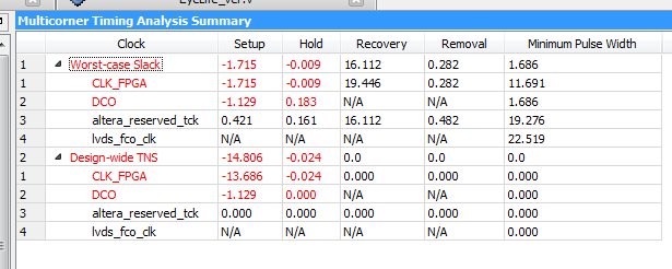
I am trying to figure out how bit clk and fclk are related on the LM96511.  I am trying to include the FCO_CLK in the SDC file but I don't know why lvds_fco_clk is showing as N/A.  Any guidance or documentation on how to setup these clocks?


Regards,

  • Hi Rob,
    It is not clear what you've shown (Multicorner Timing Analysis) and what LVDS_FCO_CLK are (as these names do not correlated to any pins / functions on the device) !?
    Are you working with the LM96511 IBIS model?

    Please clarify.

    Regards,
    Hooman

  • Hi Hooman

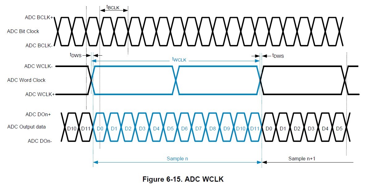
    I am trying to figure out the same issue. The specific signals can be found on page 24 of the LM96511 Data sheet.

    The signals of interest are ADC BCLK (bit clock) and the ADC WCLK (word clock). Once the BCLK has been used to deserialize the LVDS data into the FPGA the word clock is used to capture the complete word (or data sample) on the sample boundary.

    Typically it will be done synchronously with respect to the bit clock. There is however no identifiable relationship in the datasheet between the BCLK and the WCLK so there is no deterministic way to do this without meta-stability occurring.

    Is this relationship published or available?

    Many thanks

    Steven
  • Hi Steven,

    Do you mind marking up this timing diagram to state what is the exact timing between ADC BCLK and ADC WCLK you are looking for that is not in the LM96511 datasheet?

    Regards,

    Hooman

  • Hi Hooman

    The only relationship shown is tDWS (Data edge to Word edge skew). 

    The real issue here is how to use the WCLK in the FPGA to frame a complete sample (LSB to MSB). We have coded the LVDS deserializer to use to BCLK to capture the data. So all internal parallelized data is synchronous to the BCLK. SDC (Synopsis design constraints) scripts are created to direct the Quartus fitter to place and route the logic so it meets the timing requirements of these signals from the ADC.

    There is no defined relationship between the BCLK and the WCLK.  Thus there is no deterministic relationship between the two signals and we have to treat WCLK as if it is asynchronous to the BCLK. If there was a guaranteed relationship (as there is between the data and the BCLK) then we could guarantee valid setup / hold timing of WCLK with respect to DCLK. This would make syncronizing WCLK to BCLK possible. This is important because we use a sync'ed delayed version of WCLK to capture the input data in a shift register on the LSB / MSB boundary.

    Thanks for the assistance.

    Regards

    Steven

  • Hi Steven,

    My understanding of this device interface is that the WCLK is just another data line that is used to indicate the frame of the data so that the digital sample can be re-constructed AFTER the data has been passed into the FPGA core. I do not think it should be used as a deserializer frame clock. I think the WCLK should have an identical digital receiver/DESER as all the output data lines. I would assume that the tS and tH would apply to the WCLK as well. The tDWS spec is specifying the worst case differences between the WCLK and a data line.

    Regards, Josh