This thread has been locked.

If you have a related question, please click the "Ask a related question" button in the top right corner. The newly created question will be automatically linked to this question.

AFE5808 - strange artefacts

Other Parts Discussed in Thread: AFE5808

Hello,

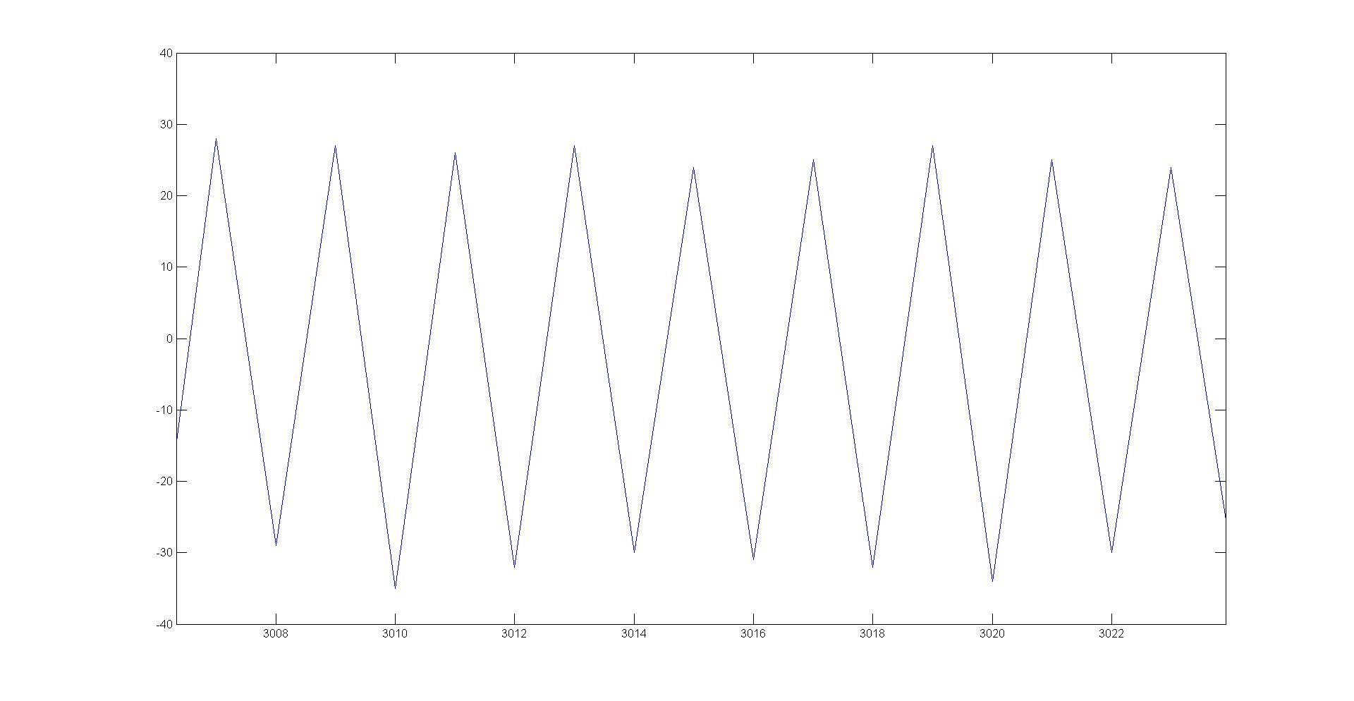
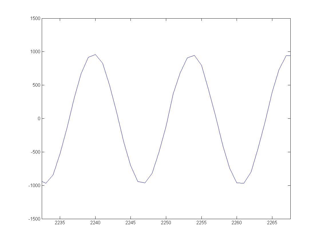
One of our customers is working on Analyzer equipment, using the AFE5808. The customer is experiencing some strange artefacts during the measurements. When using a 5mVpp sine wave 1.8MHz, a sine wave is seen (visualization using Matlab). See the attached image “Sinus 1.8 Mhz 0.005 Vpp.jpg#. When the input is terminated with 50Ω, noise (modulated by the clock, or alternating around zero every clock cycle). See the attached image “Alternating noise with 50 Ohm termination.jpg”.

Attached an image of the AFE settings as well (“AFE Settings.jpg”).

What could be the cause of this artefact/problem. What can be done to solve it?

If you need more information, please let me know.

Regards,

Meir.

  • Meir,
    It seems from the noise plot, that you could be skipping or missing some of the LSBs. Can you confirm that you have all 14 bits in your data? Please use a test pattern mode, like ramp, to confirm that the digital data link is correct. Also, I notice that you have Digital Gain enabled, reg: 3[12]=1. Can you try without that?
    Chuck Smyth
  • Hello,

    I will check with the customer if he can confirm on your question. In the meantime the customer informed me about the following:

    They measurements at the inputs of the ADCs (25MHz clock frequency, which can be switched on and off), using a special pre-amplifier (used at EMC near field measurements) and a oscilloscope with spectrum analyzer functionality. A 50MHz signal was clear visible, coming out of the ADC, and within the input range. The base frequency was not visible. When switching off the ADC (with the clock still on), the signal disappeared.

    Is it possible that, even that there is a low pass filter, this signal could be measured (it comes out of the ADC)? This could lead to the alternating signal, as seen in the previous send pictures, as added to the signal.

    Regards,
    Meir.

  • Meir,

    Can you please describe the device pins at which they are measuring 25MHz or 50MHz?

    The alternating signal is unusual and probably not caused by this phenomenon.


  • Hello Again,
    Thanks for your answer.
    The customer measured 50Mhz at input of the ADC after switching the ADC on. Switching off the ADC or switching off the clock removed the problem completely. There was no 25MHz. He measured this using a special preamp he normally uses for EMC probes and a Lecroy scope in spectrum analyzer modus.
    They don't think they are missing bits due to the following:
    - missing a bit would result in abrupt jumps of the signals
    - If it was a deserializer problem the result would at least change now and then: 0 would become 1 and vice versa. Our problem is extremely regular and therefor seems fully clock related.
    - When looking at the noise it is clearly centered around zero. This would imply that the sign bit (they are using two's complement) would be erratic (not one of the LSB bits) but if you look at the measured sine wave you will see that nothing is wrong with that.
    - When looking at the sine signal they see the same modulation on 4 chips, all 32 channels when terminated with 50 ohm.
    - The 50Mhz signal is coming from the chip, if it is measured by the ADC with 25MHz then this will result in a + - modulated signal which is locked to the clock.
    - They looked at the ramp test signal but they are only able to measure 4096 samples. Results looked good. They are currently not able to do new measurements as they on their summer holiday.
    I hope this info, will help you, please ask extra questions if needed.
    Regards,
    Meir.
  • Hi Meir,

     I am increasingly convinced of your hypothesis that it might be analog.  I need a few more pieces of information, though:

    1. I want to verify that the issue is indeed an analog issue and not a digital capture issue:
      1. Try another test pattern like toggle mode to verify that all bits are working as expected.
      2. Vary the gain and capture data to see if the oscillation is amplified.
      3. Is it possible to remove or power down in the ADC input clock and not power down the ADC?


    2. Layout Concerns

      1. Are the analog and digital grounds combined or separate?
      2. Do you see the same oscillations on the analog power supplies going into the device pins, AVDD_5V, AVDD_3V.
      3. You mention that you are probing at the ADC input.  Do you mean the AFE input? Which pins, INP, INM or ACT?
      4. What are the bypass capacitors on the power supply pins and how many?  Are the caps close to the pins.
      5. For the INP and INM pins,  are there any vias going through a ground plane or near a PS plane?
      6. Is there sufficient isolation of power planes (clearance)?
      7. How are the power supplies isolated from each other.

    My suspicion is that the second harmonic is generated in the ADC and feeding into the AFE inputs through a GND, Power or close proximity plane.


  • Hello,

    I hereby send you the answers on the questions you have asked.

    The customer suspect that the artifact is created between the LNA and the PGA.  

    The measurements on the power supplies, are very difficult in the sense that their FET-preamp has a DC input. So they need to use a capacitor to make it AC.

    Regards,

    Meir.

    Response Texas Instruments.docx

  • 1.2     Increasing the gain in LNA 18dB to 24 dB adds more external noise to the signal (modulates it) / digital gain from 1 to 6dB increases signal / changing VCA attenuator does not change amplitude

    Do you mean that an LNA gain increase amplifies the artifact, or just the random noise?  The artifact amplitude does not change with VCAT change? 0-40dB?  This implies the artifact is introduces between the VCAT and the PGA.  Does increasing the PGA gain from 24dB to 30dB amplify the artifact? Please power down LNA, VCAT and PGA in that order until the artifact disappears, reg 0x35. 

    The layout seems ok,  it would be good if you could probe the AVDD-3.3V supply for the artifact.  This supplies the PGA.