This thread has been locked.

If you have a related question, please click the "Ask a related question" button in the top right corner. The newly created question will be automatically linked to this question.

Clock input to CIS sensor from LM98722 AFE's CCD timing generation

Other Parts Discussed in Thread: LM98722

Hi,

I am using Contact image sensor in my application, I am using LM98722 AFE to interface CIS sensor, i need help in CCD timing generation in LM98722 for providing clock signals to my CIS sensor..

I need to give 4 MHz clock input and 3.6 KHz clock input to my CIS Sensor, how can this two clock frequencies can be generated from LM98722 AFE CCD timing generation.

Thanks in Advance....

Regards,

Gokuleswaran R

 Design Engineer

  • Hi Gokuleswaran,

    We'd need to see the timing diagram of the clocks you need for the CIS to see if the LM98722 is capable of generating them.

    Can you provide that?

    Regards,

    Hooman

  • Hi Hooman,

    Thanks for your Reply,

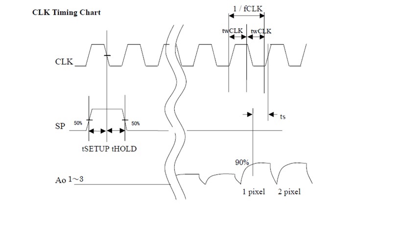
    As for the information required for you, i have attached the timing diagram for your reference.

    Note:

    Clock Frequency – 4 MHz

    Clock Duty Cycle – 50%


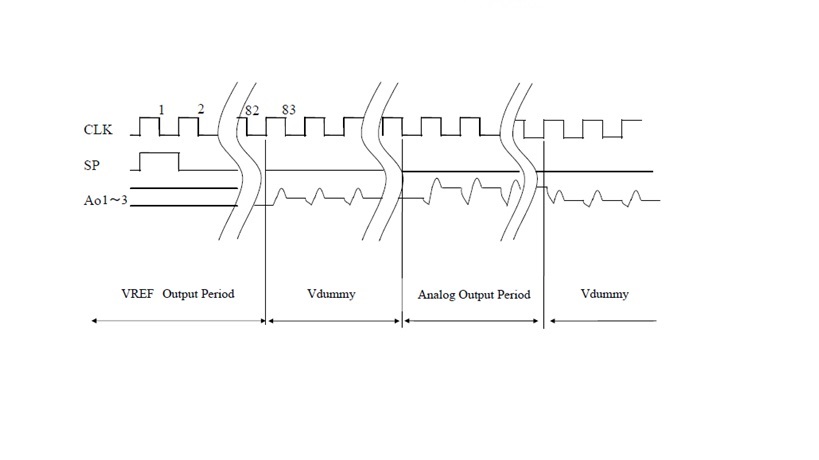
    Data Output Timing Chart:

    After turning on the SP pulse, the analog output starts from the setting up point of 83 clock pulse.

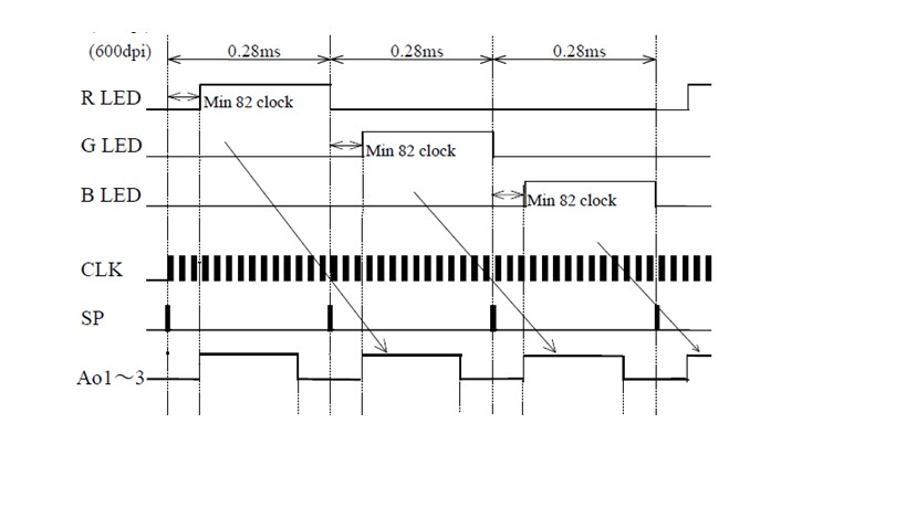
    Reading Colour Document:


    Thanks....

    Regards,

    Gokuleswaran R


  • Hi Gokuleswaran,
    I got the following details for your specific timing requirement from another colleague and I've copied it below.

    See the programming sequence in Section 7.5.1, along with Table 6 and Figure 41 for a lot of details related to these settings.

    • Mode 3 for 3 input signals from CIS – Page 0, Register 2 Bits 7:6 (value [11]).
    • Set for Master Mode (AFE determines system timing to sensor) unless it needs to be synchronized to some other system (motor drive?). In that case use Slave Mode and drive SH_R input as needed to trigger the start of each new line. Master Mode: Page 0, Register 0, Bit 1 = 1.
    • CISa (CISb could also be used) – Page 2, Register 10h, Bits 4:3 [10] for CISb).
    • Three line color sequence – Page 2, Register 10h, Bits 1:0 [10].
    • Line length set to be around 1120 pixels to ensure all pixels clocked out. (Calculation gives line length of 1111.1111 pixels). (Page 3, Registers 0x0D and 0x0E)
    • Active/White pixels start at approx. pixel 83
    • Active/White pixels end depending on number of Analog output pixels not specified, some value around 1111 or so pixels).
    • SH1 (Red Lamp), SH2 (Green Lamp), SH3 (Blue Lamp) On pixel set to be >83 pixels from start of line.
    • SH1, SH2, SH3 Off pixel set as needed to achieve desired brightness of R,G,B lines.
    • Configure CP output to toggle low/high/low once during each of the 3 SH intervals
    • Configure CP to be always low during the line
    • Configure PhiA to toggle Low/High/Low/High once during each of the SH intervals
    • Configure PhiA to toggle Low/High once per pixel (50% duty cycle)
    • Set clock mode to Pixel Rate input clock (4 MHz)
    • Set data to LVDS mode and enable data outputs
    • Set CP, PhiA, SH1, SH2, and SH3 unlock states as desired, when the device is being programmed and is inactive these will be the logic levels on these outputs
    • Enable CP, PhiA, SH1, SH2 and SH3 outputs as Active, Timing, Not Inverted.

    Hope the information above is helpful.

    Regards,
    Hooman
  • Hi Hooman,

    Thanks for the information, I hope this information help us great to continue with our task, and once we achieved the output I ll intimate you.

    Thanks Again......

    Regards,

    Gokuleswaran R