This thread has been locked.

If you have a related question, please click the "Ask a related question" button in the top right corner. The newly created question will be automatically linked to this question.

ADS7846: Inexplicable burnout

Part Number: ADS7846

Hi

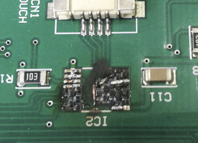
We use ADS7846 in our project from several years. Recently, we have received, to repaire it, some circuits with ADS7846 completely burned without any apparently cause. The packaging was been deformed because of overheat or explosion. Also pcb and traces under the chip are burned. All the rest of circuitry, display and touchscreen are functioning.

In the past, also other chips were failed, but never in this too energetic way.
Which could be the cause?
Is it possible introducing some protection to avoid such fail?
Thanks for any help.
Regards

  • Pietro,

    1. Did the device fail on initial power up or did it fail during normal use.
    2. Are these returns from the field? What percentage of devices have this problem?
    3. The likely cause of this problem is ESD/EOS damage on the input. It is possible that this damage could cause the internal ESD absorption device. A detailed discussion on how this happens on amplifiers is given in the links below. Although this material was written for amplifiers it pertains to ADC input as well.

    https://training.ti.com/ti-precision-labs-op-amps-electrostatic-discharge-esd?cu=14685

    https://training.ti.com/ti-precision-labs-op-amps-electrical-overstress-eos-1?cu=14685

    https://training.ti.com/ti-precision-labs-op-amps-electrical-overstress-eos-2?cu=14685

    https://training.ti.com/ti-precision-labs-op-amps-electrical-overstress-eos-3?cu=14685

    1. The most common protection scheme is to use external Schottky diodes (BAT54S is a common choice) to either supply on the input of the ADC. The document below shows this protection scheme on the input of an ADC.

    http://www.ti.com/lit/an/sbaa245/sbaa245.pdf

    I hope this helps.

    Art Kay

  • Hi,

    Thanks for your reply.

    I answer your questions immediately:

    1. The device fails during normal use. We have had the opportunity to investigate better how the fail occurs. The cards with destroyed chips come from the same installation. So this leads us to think that there may be some problem in the particular installation, but at present we cannot go to check. The user reports that, upon occurrence of the fault, he takes an electric shock. In other installation, where the chips were failed, they didn't burn in this very strong way; so it's possible assume that there could be a problem with the ground potential in this particular installation or is this assumption completely foolish?

    2. This installation has been made recovering an old system from another installation that had worked for several years without any problem. Two devices are returns from the field; both were replaced with new devices, and, after two weeks, both new devices have failed in the same way.

    I've attached two sample photos.

    Thanks for any suggestions

    Regards

  • Pietro,

    Sorry for the long delay.

    1. When you say that the user receives an electrical shock, I wonder what voltages are applied to this device. Is something breaking down or miswired that applies a high voltage to this device? I agree with you that it may be that there may be a problem with the ground potential or some other kind of miswire. If the normal voltage applied to the device is inside the absolute maximum ratings (Vcc+0.3V) you should never feel an electrical shock.
    2. I’m not sure that I understand your point 2. I believe that you are saying:
      1. a system was out in the field for several years and didn’t have any problem
      2. At some point the hardware was returned and re-worked. Did the hardware have EOS damage?
      3. When the new hardware was returned to the field the devices had catastrophic failure.
      4. I suspect that when the devices were returned to the field they were miswired.

    Best regards,

    Art