This thread has been locked.

If you have a related question, please click the "Ask a related question" button in the top right corner. The newly created question will be automatically linked to this question.

TPS54290: Not getting Out2 as expected

Part Number: TPS54290

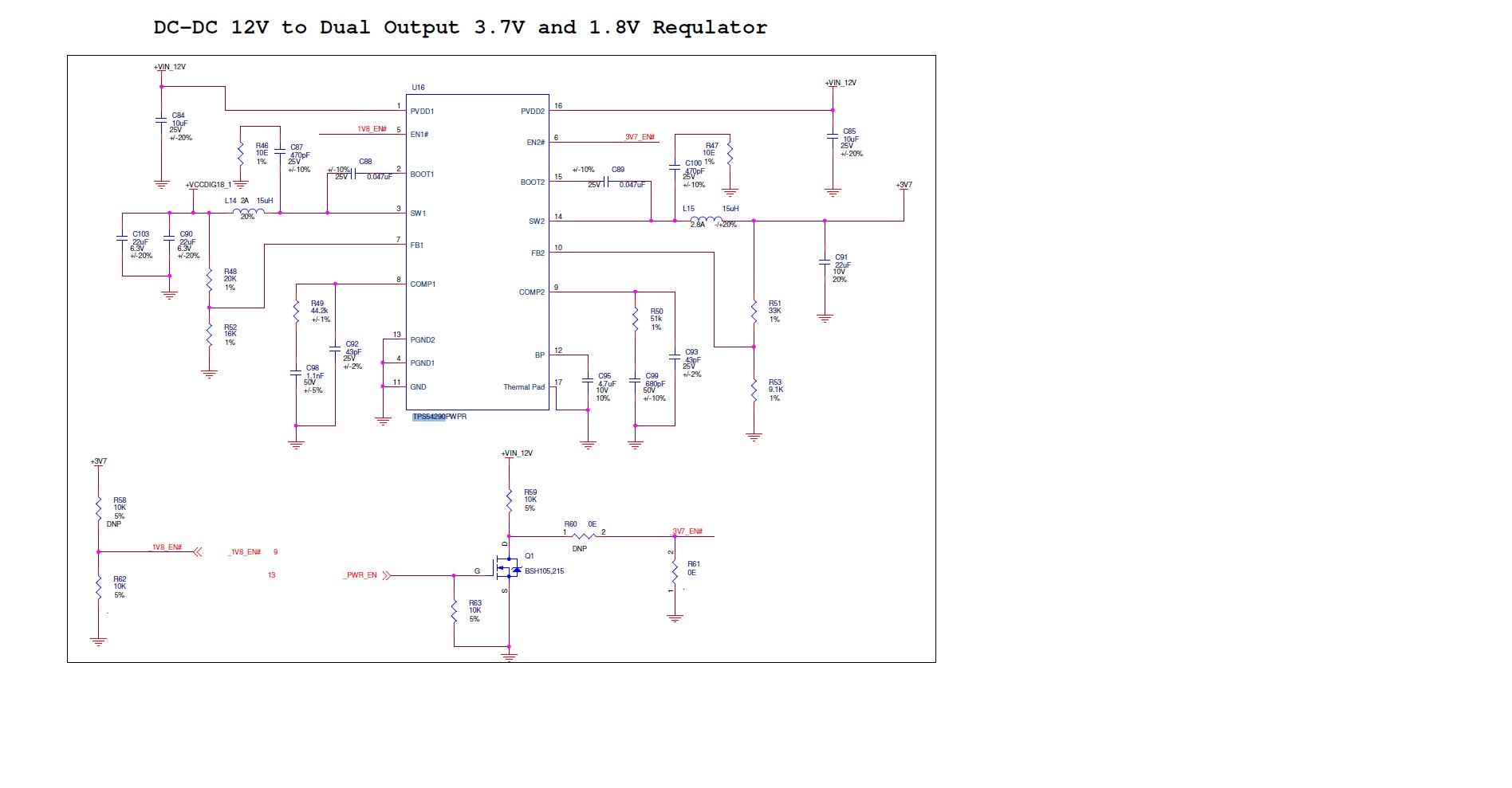
Hi,  We are using TPS54290 in our design and using it as Dual output source ( 1.8V and 3.7V respectively) .

PVDD1 and PVDD2 are shorted and fed by 12V supply.

Default EN1 and EN2 are pulled down. 

After turning on input PVDD1=PVDD2 = 12V . We are getting Out 1 around 1.48-1.9V  on 5 boards we tested( should be 1.8V as R1 /R2 at FB1 are 20K/16K) .

But major issue issue is with Out 2  . we are getting around 1.77V - 2V range on 5 boards we tested.  (should be 3.7V as R1 /R2 at FB2 are 33K/9.1K) .)

Is there any sequencing required for EN1 and En2  ( EN2 should come before EN1) in case when we have PVDD1 and PVDD2 tied together?


  • Can you post your actual schematic?  Can you provide waveforms showing SW1 and SW2?  You should be able to assert both EN simultaneously.  Make sure the PVDD rise time is faster than the SS time.

  • Attached is schematic for your reference. Please let us know if you see any issue.
  • Looks like EN2 is pulled down with 0 ohms while EN 2 is pulled down with 10 k. I would recommend 0 ohm for both, but that is probably not your issue. I'll need to see the waveforms. Sw1 and SW2 for sure and maybe VIN with Vout 1 and Vin with Vout 2 to start with. Make sure we can see individual pulses on the SW1 and SW2 waveforms.
  • Hi John, yes we did try pulling down EN1 directly to GND. But it doesn't work. We disabled the OU1T1 (1.8V) by Pulling EN1 high but still see same issue with OUT2 ( 3.7V).
    Attached are snapshot of SW1 and SW2 .
  • Your 1.8 V switching waveform looks more or less normal except that it is regulating to about 1.45 V rather than the desired 1.8 V. the 3.7 V waveforms are totally abnormal. What is your PCB design like?
  • Hi John. in our board we are feeding 12V DC as input to TPS54290 and generating 1.8V ( max load current will be 750mA) and 3.7V ( Max load current will be 415mA. 1.8V is directly given to controller IC . But 3.7 V is fed to 3 LDOs to generate 3.3V and which is given further to rest of the IC modules on our board. Default we made EN pin of TPS54290 as Low so that both can be enabled by default.
    Is max output capacitor value can affect it. Can it create start up problem as mention in datasheet . Please let us know if you find any issue with TPS54290 schematic I Shared with you.
    Also We disabled all the LDOs on 3.7V path and still facing same issue. The only difference is now the Output fluctuating between 1.7V to 2.3V . Previously it was around 1.7 to 1.8V only. Also we isolated the load from 1.8V output and didn't observe any improvement.
  • I did not see anything specific on your schematic. 1 x 22 uF or 2 x 22 uF should not be viewed as excessive capacitance in my opinion. I think I would cut the etch (or lift or remove components) to all loads on both rails, to see if your circuit can start up normally. Alternately, you could get a TI EVM with a known good layout and modify it to replicate your schematic. It is possible that your pcb layout is not good or you have interaction with other circuits. Even though your 1.8 V rail switching waveform looks "normal" it is not the correct duty cycle for your 1.8 V output. The 3.7 V rail looks unstable or maybe current limited. Maybe your input voltage supply is current limited? As you may have noticed, troubleshooting over the internet is not particularly efficient. Do you have a local FAE you typically work with?
  • Thanks John!
    What is the Output capacitor value which we consider as excessive?
    As the 3.7V Output of TPS54290 goes to 3 LDO and each has one input capacitance ( 1 uF, 10uF, 2.2uF respectively) at their input so effective Output capacitance will be around 35uF. Similar way for 1.8 V effective output capacitance will be around 56uF.
  • SW_OUT_COMP_Waveform.zipHi John,

    We removed all load on our board from OUt2(3V7) and OUT1(1V8). And still see same issue. We also powered rest of the design from external DC bench power supply and it works fine. So look like issue with our TPS54290 design.

    I am attaching again the SW and OUT waveform of 1V8 and 3V7 volt rails. Please let us know if you found any thing from that .

    Also we are suspecting now the Compensation ckt of TPS54290 on COMP2 pin.   We removed C92 and C93 from our design and with Out2(3V7) disabled. We are able to get stable output at OUt1 (1.73V) . But if We enable 3V7 (OUT2) then again we see same oscillating output at 1V8 and 3V7 outputs. Now we are suspecting if C99 value is assembled wrongly and affecting the design.

  • Looking at the timing of the SW node, you are definitely entering hiccup mode (30 msec for TPS54290). Also, your switch node voltages are only about 5 V, not the 12 V you show on the schematic. Can you check that you are actually getting 12 V at the input PVDD1 and PVDD2?
  • Sorry I forgot to mention that the latest waveform are taken with 5V as input to PVDD1 and PVDD2
  • From a start up perspective, you want to limit the capacitance so the converter does not reach current limit.  You are charging up the output at a constant rate so the maximum capacitance is:

    Cmax  = I(CL) * t(SS) / Vout

    Where I(CL) is the current limit and t(SS) is the soft start time

    56 uF is going to be way less than that.

    I think you may have stability issues that are allowing the duty cycle to be large and allow the current to ramp up unnecessarily high.  At this point I think I would start with the known good layout of the EVM, then modify the EVM to match your design.  I would also carefully go back through your design equations to make sure everything is correct.

  • I went thru the calcs for compensation for 3.7 V. Try R60 = 150 k, C90 = 1500 pF, C93 = 15 pF. Let me know if this works better.
  • I ran your designs in pspice this morning.  They are not stable.  How did you calculate the compensation?

  • Ignore my previous compensation recommendation. Here is what I suggest you try:
    R49 = 10 k
    C98 = 6800pF
    C92 = 22 pF
    R50 = 10 k
    C99 = 4700pF
    C93 = 22 pF
    Hopefully I have the reference designators correct. They are pretty small in your schematics. These values are for the compensation components. Let me know if these work for you.
  • DC_DC_Buck Regulator_Components_Calculations_updated.xlsx

    Thanks John!

    We will try these values.

    Just for curiosity. How these values are calculated We calculated earlier values as per attached sheet. Were we missing something in calculation?

  • I did not calculate them. I just looked at the pspice avg sim results and did it visually. I have done so many now that I seldom need to do any calculations. The caveat is that this assumes the model is correct. Our group inherited support for this part. We were not involved in the development. Anyway, give it a try and see if it helps.
  • slum164 (4) - autosave 17-12-07 10_55.TSCSure we will give it try.

    Also just to mention here, We designed it to support Input voltage from 4.5V to 13.2V. Is that make any difference in your calculation.

    We simulated the design here in Tina Spice and couldn't see any issue . Attached is spice model we simulated before finalizing design.

  • At this point, I am just trying to get you up and running. Please use 12 V as your input for now.
  • Thanks John!
    After replacing the compensation component values as you suggested TPS54290 s up now. It is working with both 5v and 12V input supply.
    But still we really have no clue that how these new values are selected as when we calculated the values as per datasheet , we got different values and TINA spice model was working as expected with those values while simulating our design. Just for our knowledge can you please see the attached sheet and let us know here we went wrong while calculating the values as it will surely help us in any future design.
  • I am pleased that my recommendation worked.  Sometimes power supply design is a mixture of both science and art as I did not use any equations to design the compensation network.  I don't see your attachment.  If you can provide it I may be able to give you some feed back.

  • 0743.slum164 (4) - autosave 17-12-07 10_55.TSC8473.DC_DC_Buck Regulator_Components_Calculations_updated.xlsxSorry i didn't mentioned correctly, it was attached in one of my previous reply. I am attaching it again here.

  • The TINA model you attached is for transient response and The Excel file will not open. Since the values I provided previously are working properly, I will close this as resolved.

    Thanks,
  • Hi John,

    Yes with the  value you provided, it is working. But we wanted to know where we went wrong in calculating the compensation network components values and how these values arrives.

    It will be really helpful if you can go through the excel and see if we did something wrong. We couldn't find it from our end . And if we leave it now,  it can again be repeated in future design too if not corrected.

    Thanks & Regards,

    Bhupendar


  • Bhupendar,

    I have reviewed the spreadsheet you sent.  It had an invalid character in the file name that prevented me from opening  it, but renaming fixed that.   I went thru every calculation in detail and did not find any errors.  I also used the resulting component values in pspice.  Pspice predicts output 1, Fco = 57 kHz, PM 36 deg.  Output 2, Fco = 68 kHz, PM = 13 deg.  Both of those are low especially output 2.  As I may have stated previously, we inherited support for TPS54290 from another group, so I do not know who derived those compensation equations and spreadsheet.  They most likely work well for some scenarios, but not for your case.  I will note this issue to our management to see if someone can be assigned to update it.

  • Thanks John!

     Appreciate your support on this issue.

    It will be great if you can route us to the right contact who can help us to find the right way to calculate compensation values for TPS54290.

    Thanks & Regards,

    Bhupendar

  • John,

    Thank you for supporting Bhupendar on this issue. He is working on my board design and the TPS54290 looked like an ideal part for our prototype but we will not be able to use it for production or any future design if we cannot figure out how to calculate the correct values for the compensation circuit. Please let us know if you can find the right person at TI to figure this out.

    Thanks,
    Dave Urban
  • Hi Dave,

    My group inherited this part during a re-org. I would like to fix all this, but it is not a simple task to reverse engineer those equations, re work them, then validate the new design procedure for several corner cases, rewrite the excel tool and update the datasheet. My queue for a project of that scale is full up at the moment. As I may have commented earlier, I personally use and recommend pspice modeling for compensation design, which is supported for TPS54290. Will that work for you? I can arrange a tutorial if you like. Let me know, I can set something up.