This thread has been locked.

If you have a related question, please click the "Ask a related question" button in the top right corner. The newly created question will be automatically linked to this question.

LMZ31710: LMZ3170 layout

Part Number: LMZ31710

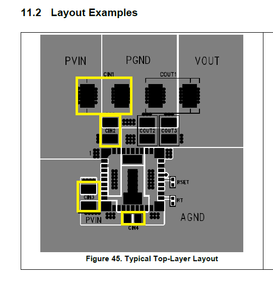
Hello I am designing in an LMZ31710 for my next PCB design. I am reviewing the recommended layout and I notice in figure 45 of the datasheet there is a cap marked cin4. I do not see any reference to cin4. Can you clarify this capacitor and its value please.

Regards,

Guy

  • From the layout, the Cin4 should be a high frequency bypass cap between VIN and ground, for pin 11/12 and pin 20/21, on this side of the module. It should be a low capacitance ceramic cap, around 1 uF should be fine. The voltage rating should be >150% of VIN.

  • Yang is correct, C4 is the high frequency bypass capacitor. The recommended value in the datasheet is 0.1 uF. Just for your reference, the other capacitors are:
    C1 = electrolytic input capacitor
    C2 = ceramic capacitor at the PVIN pins 1, 39 and 40
    C3 = ceramic capacitor at the PVIN pins 11 and 12.
  • Hi John and Yang. Thank you for your replies.

    I am still a bit confused. As you can see in the layout in figure 45 there are four capacitors not three, CIN1 through CIN4. There is no mention of CIN4 in the datasheet other than in figure 45.

    So just to be clear as I have understood it from both of your repsonese and please see copied attached reference layout for these comments

    CIN1 = 100uF  input capacitor

    CIN2 = 47uf ceramic  pvin pins 1,39,40

    CIN 3 = 0.1 uF ceramic pvin pins 11 and 12

    CIN4 = 1.0 uF ceramic pvin 11,12 and GND pin 20/21

    Regards,

    Guy

  • I agree, it may be a little confusing. The layout guidelines do not necessarily apply specifically to any of the design examples. Based on the the layout shown, I agree with Yang that C4 is the high frequency bypass capacitor. While he suggested C4 = 1 uF, the datasheet specifically recommends 0.1 uF for the HF bypass. While I do not directly support the LMZ31710 module, it is a good idea to locally bypass the PVIN pin to GND. Since LMZ31710 has the PVIN pins located in two distinct locations, I would place a capacitor near each. In addition to the electrolytic C1, the datasheet recommends a minimum of 44 uF of capacitance fro PVIN to GND. You have to take into account the dc bias characteristics of ceramic capacitors. As the applied voltage increases towards the rated voltage, the actual capacitance can decrease drastically below the nominal capacitance. You may want to place 47 uF at both C2 and C3 location. You could alternately place 2 x 22 uF at each location. It all depends on the derated value. Just be sure it is greater than 44 uF. In the layout example VIN is tied directly to PVIN. If you use a separate VIN voltage, bypass that locally at pin 3 with 4.7 uF. Hopefully this will clear it all up. If not the normal support person should be back after the holiday. Let me know.
  • Hi John and Yang, thank you for your input. I have another question regarding the layout. In the data sheet it shows an island for the PH pins on all inner layers. How critical is this to have these pins this isolated? I have a 12 layer PCB, should this island be propagated through all the layers?

  • Hello Guy, 

    I believe the island of PH was propagated to all the layers for thermal dissipation purposes. It will help with getting some heat out of the device. The trade-off of propagating the PH node to other layers is potential noise coupling. I would suggest forcing more clearance between the PH island and nearby copper. This would minimize any capacitive coupling to the nearby nodes. The top and bottom layers will be the most effective for getting the heat out to the ambient. Perhaps you can use copper islands on the outer layers so that you still get the thermal benefit and minimize potential noise coupling.

    I will also contact the Apps engineer who worked on this board. He may have some more suggestions. 

    Cheers, 
    Denislav