This thread has been locked.

If you have a related question, please click the "Ask a related question" button in the top right corner. The newly created question will be automatically linked to this question.

TPS63030: Converter is not responding to ENABLE signal

Part Number: TPS63030

Dear TI,

The problem is that TPS63030 converter is not responding to ENABLE signal if we want to turn off device. Some devices get this after a few on-off cycles, but usually device can work correctly many weeks. During this time converter is enabled and disabled from tens to hundreds, sometimes thousands times. One time it just stucks in ON state and draws the battery to empty in a week. Approximately 10% of devices are affected by this issue.

After it stuck there is no reaction to state changes on ENABLE pin. The only way to turn it off is to completly remove power from device and apply it again. Usually, after first stuck, device stucks every time it is enabled. Some devices goes to completely unregulated state, giving 6.4V output (no matter the input) just after it is powered. Only a few devices after first stuck and power off/on recovery enters normal operation.

Design details

Both schematic and layout are very close to reference. Only difference is additional 100R resistor between VIN and VINA and 2p2 capacitor in parallel to upper resistor in feedback divider. Load is GSM module with 0.14F supercap in parallel.

Vin: 3,3 - 3,6V
Vout: 3,8V
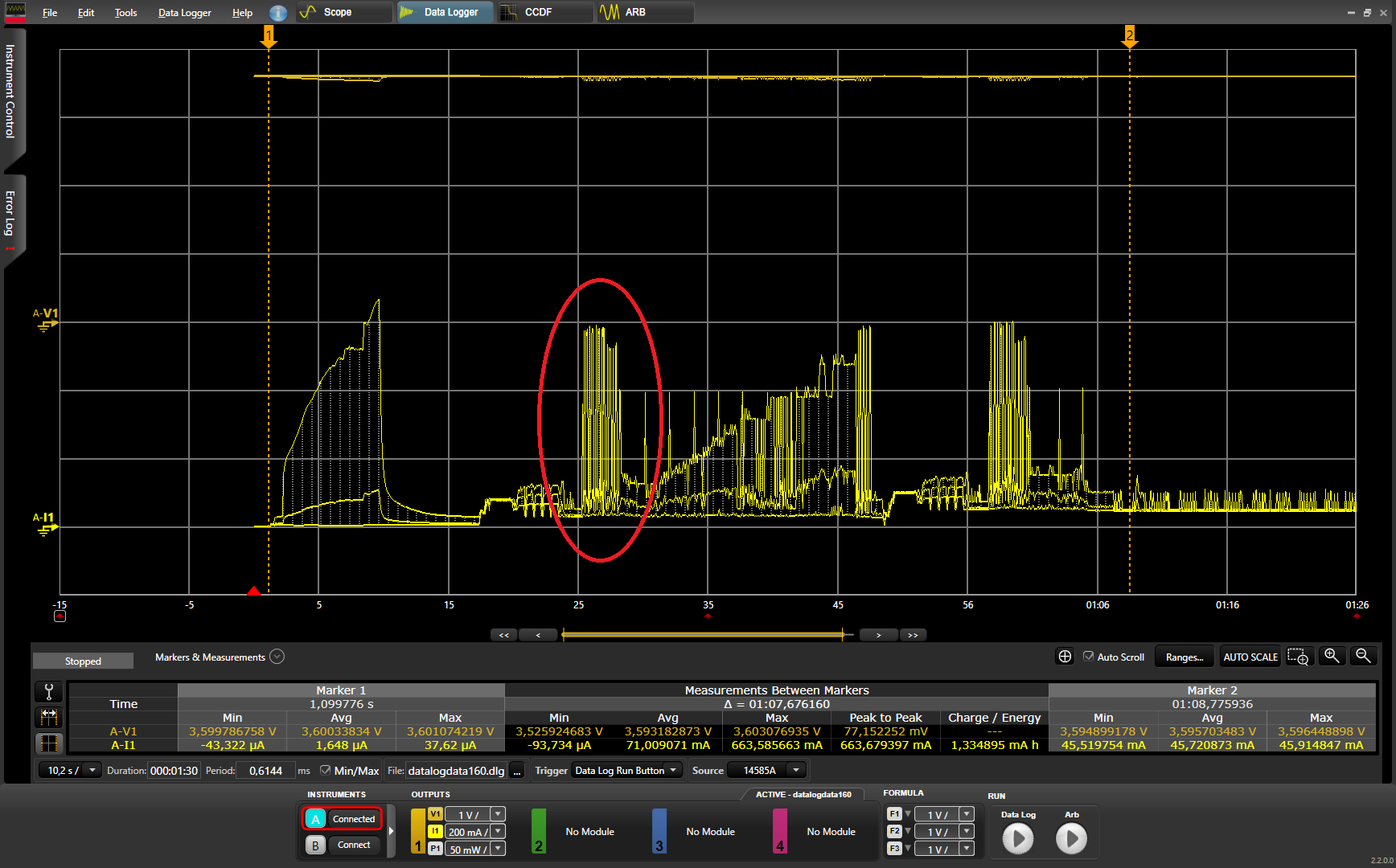
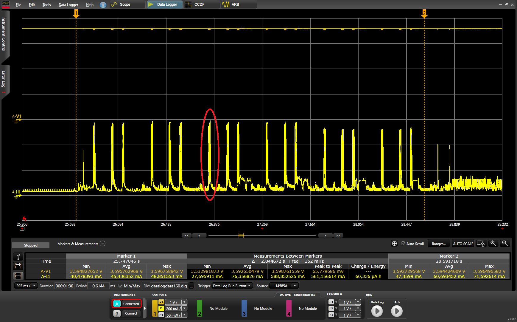
Iin: avg 80mA, 700mA peak (peaks are 577us long with 4.615ms period during GSM transmit burst).

The only untypical thing that we do using IC is supercap charging procedure. If it is empty we are switching regulator ON/OFF using ENABLE pin to not allow battery current to reach more than approx. 0,5A. At the fastest stage device is 1ms ON / 8ms OFF.

Here are input current profiles (200mA/div):

Thank you in advance for your help.

Best regards,

Marcin

  • Hi Marcin,

    I don't find an explanation for this behavior on he schematic and layout, they look fine to me.

    1. Could you clarify this statement :
    "The only untypical thing that we do using IC is supercap charging procedure. If it is empty we are switching regulator ON/OFF using ENABLE pin to not allow battery current to reach more than approx. 0,5A. At the fastest stage device is 1ms ON / 8ms OFF."

    2. Is the super cap being charged for 8ms and discharged in 1mS ? As this is connected to VIN, I am a little confused on the Vin range for the converter

    3. Regarding the "input current measurements", Where is this measured exactly (on the schematic)? What is the load profile? Could you retake this with VIN, Vout and Iout on the same plot?

    4. Could you exclude any soldering issues here? I am asking this because 10% is pretty high, since when is this design in production?
  • Hi Marcin,
    were you able to find the root cause?
  • Hi Sabrina,

    No, I didn't find anything more. 

    Regarding your questions:

    Ad 1. We don't want battery current to exceed 0,5A, so we are turning off converter each time its input current is reaching this value. So, there is some period when converter is on for only ~1ms and then off for ~8ms. I know It's not too elegant, but can it lead to damage?

    Ad 2. Supercap is connected to Vout.

    Ad 3. Current measures were taken at input connector, J5 on the schematic. I will try to take aditional plots.

    Ad 4. We checked that this is not a soldering issue.

    I'm sorry for late answer, I was out of office last week.

  • Hi Marcin,

    Thanks for the answers, I don't think this would lead to a damage.

    I would some more details:
    "not responding to enable" , what does it mean for VOUT ?
    what is the current consumption at no load once the device is stuck in this condition?

    I am waiting for the additional current measurement with VIN, VOUT and IOUT, to understand further what could be the root cause.
    It would help to have a plot for a "good Unit" and for a unit that is "not responding to enable" to compare both behavior with the same operating condition.