This thread has been locked.

If you have a related question, please click the "Ask a related question" button in the top right corner. The newly created question will be automatically linked to this question.

BQ24640: Minimum recommended PAD size for RVA ( S-VQFN-N16) package?

Part Number: BQ24640
Other Parts Discussed in Thread: LM5085

Team,

Customer has some PCB manufacturing requirements that are imposed by the application and PCB manufacturer.

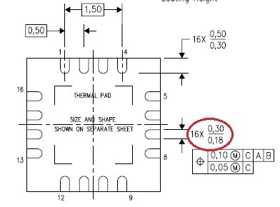
For the BQ24640RVA the PCB manufacturer need to use a PAD width of 0.2mm (see picture below).

1)Can a 0.2mm PAD width be used for this package? Can a reliable soldering and long term device operation be garanty with this width?

2) Do we plan to have more industrial friendly package for the BQ24640 device? Or to have other supercap charger device in other package in the future? Any timeline?

3) I have seen the below FAQs page for QFN:
http://www.ti.com/support-quality/faqs/qfn-son-faqs.html

The "QFN/SON PCB Attachment -SLUA271A" app note does not seem to be listed there.
Is this app note relevant for S-VQFN-N16 too? Or is there a document specific for S-VQFN-N16?

Thanks in advance,

Anthony

  • Hello Anthony,

    Regarding 1, below is the feedback from our packaging team.

    "When customer stated that they want to use 0.2mm pad. That means they want to layout their PCB pad using 0.2mm in width.

    The nominal width of the component pad is 0.24mm. If the PCB pad width is 0.2mm, then the solder joint shape would not be optimized. It will affect the solder joint reliability, putting most of the stress to the interface between PCB pad and solder joint causing earlier than expected failure.

    Not recommended. "

    Regarding 2, could you please let us know who is the customer? What is the end equipment? What is the requirements for more "industry friendly"? This is actually our first time learned about this 0.2mm requirement. It would be really helpful if you can provide more info to help us understand this requirement. 

    Regarding 3, this is a general document. Please see the link below.

    www.ti.com/.../slua271a.pdf

  • Hi Jing,

    I´m Iñaki Larequi, the person who contacted Anthony to send the footprint request about the BQ24640.

    The reason why I want to reduce the pad width in the BQ24640´s footprint is to get 0.3mm separation between pads. I´m using this IC in a power application pcb where base cupper thickness of 105um is used. Pcb manufacturers have specified that separation value for massive production.

    In my design, I use the BQ24640 for charging a bank of ultracapacitors (4 ultracaps of 2.7V in series, max voltage < 10.8V) from a DC voltage of 12V. I define the charging current to 1 Amp as the power available in the board is limited. With that current, the charging process last about 5 minutes. Afterwards, the BQ24640 maintain the voltage of the supercap bank with a low current (0.5Amp). The charging process only happens when the whole system power up. That means that as long the grid is present, the BQ24640 works with a very low current, and the BQ24640 will repeat the whole charging process only if the grid dissapears and comes back.

    I´m aware that the reduction of the pad width affects the solder reliability and it can cause earlier than expected failure. However, the working conditions I detailed are low demanding for the IC. In such conditions, do the BQ24640 team reconsider their not-recommended suggestion?

    If their answer is still not-recommened, I would need to find an alternative part to implement the superrcap charger. In a fast look in TI portfolio, the part LM5085 (which has a bigger footprint) could be used as a supercap charger with the working conditions I described above. Any other suggestion from TI?

    Thank you
  • Hi Jing,

    This Iñaki Larequi, the person who contacted Anthony regarding the BQ24640 footprint request.

    I would like to explain a little bit more the design where the BQ24640 is used and its working conditions. The BQ24640 works as charger in an ultracapacitor bank (composed of 4 ultracaps in series, thus maximum voltage is 10.8V) from a DC voltage of +12V. This part is used in a power board with base cupper thickness of 105um. Our pcb manufacturing suppliers have defined us a minimum separation of 0.3mm between conducting elements for reliable massive production. To accomplish this separation in the BQ24640 footprint, the only way is to reduce the pad width to 0.2mm.

    The BQ24640 charges the bank at a constant current of 1Amp and once the bank voltage arrives to maximum value, the BQ24640 maintains the charge with a low current of 0.5Amp. The ultracap bank only charges at power-up of the whole system, and it only works again if the grid is lost and comes back. Therefore, the number of charging process is quite low (less than 1 per day as average).

    I´m aware of the impact in solder reliability if the pad width is reduced to 0.2mm. However, the working conditions for the BQ24640 are not very demanding. In such situation, do the BQ24640 team still recomend not to reduce the pad width to 0.2mm?
    If the feedback is to maintain a minimum pad width of 0.24mm, then I must find an alternative part for the ultracap charger. Having a fast look in TI portfolio, the part LM5085 could be an alternative. Any other part suggestion according to the working conditions I described above?

    Thank you
  • Hello Inaki,

    Thanks for the detailed explanation. My understanding is that the 0.2mm requirement is due to the base copper thickness of 105um. Is this correct?

    We cannot warrant the operation when it is out of the datasheet spec.

    LM5085 seems to be a buck controller only.  Currently, bq24640 is the only supercap charger in our portolio. We do not have an alternative solution at this moment. 

  • Hi Jing,

    I select 105um as base copper thickness for my power design. That means the final thickness in external layers is around 140um once the pcb is manufactured. Therefore, my pcb suppliers have recommended me to keep at least 300um of distance between conducting elements. In the VQFN footprint of the BQ26640, the only way to accomplish that requirement is to reduce the pad width down to 200um. That´s why I contacted TI to get a feedback about the feasibility of reducing the pad width.

    From your answer I understand that TI suggests not to reduce the pad width from the value (280um) defined in the recommended footprint. At this moment, we are manufacturing some prototypes of these board where the pad width was reduced to 250um. I will check then in a couple of weeks, depending on the results I could decide if I face the risk of reducing further more the pad width.

    In the meantime, I would like to find an alternative. It´s true that the LM5085 is a buck controller, but it offers an external current limit (through the PMOS rdson or through an external resistance). From my understanding, if a supercap bank is connected at the output of this controller, the charging current of the capacitors would be the selected current limit. It´s clear that the LM5085 would be have less features compared to BQ24640 as a supercap charger but it could work with that role. In my design, I could accept a single charging current for the supercap bank. The supercap bank is an energy back-up when the grid is lost, and the charging time is not very critical as it happens at power-up of the whole equipment. In fact, in my current design I define the value of 1Amp for the maximum charging current. That current means that the charging time would be less tan 5 minutes, an acceptable time for us. In this working conditions, do you see the LM5085 as an alternative for the BQ24640?

    Best regards.
  • Hello Inaki,

    I am not very familiar with LM5085. My only concern would be when the supercap is completed depleted, would LM5085 able to charge it up. You might want to start a separate post on LM5085 on this.