This thread has been locked.

If you have a related question, please click the "Ask a related question" button in the top right corner. The newly created question will be automatically linked to this question.

TPS54540: WAVEFORM IN SW PIN exceed datasheet SPEC

Part Number: TPS54540

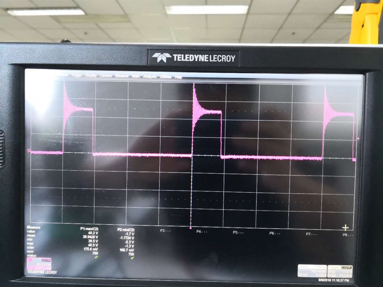
24V DC to 5V DC just do with reference design in datasheet , the output is ok ,but the wave form in SW pin as attached exceed the range in datasheet :SW –0.6 45V,the max in the waveform is -2.3V.

So if this is abnormal?    if it will lead to a failure in long time?  Thanks ~

  • Saber,

    Absolute max voltage on SW is 45V. Your ringing appears to go over 40V (not sure exactly how high). This should probably be addressed or the part may fail or have a shortened lifetime. -2.3V is also very low. The low-side FET should clamp this to about -0.6V.

    Please share your layout. Ringing is often caused by a large loop in the switch-node transient current.

    Other methods of reducing ringing (once the layout is optimized) is an RC snubber (RC in series connected from SW to GND), a boot resistor (~3-10 ohms in series with Cboot), or gate resistors (resistors in series with the gates of the FETs). These are all at the expense of efficiency so it's best to get as good as you can with layout alone.

    -Sam