This thread has been locked.

If you have a related question, please click the "Ask a related question" button in the top right corner. The newly created question will be automatically linked to this question.

TPS65916: TPS65916 Test problem

Part Number: TPS65916
Other Parts Discussed in Thread: TPS65196

Hello:
I would like to ask some questions:
1. What are the reasons for short-circuiting SMPSX_IN and SMPSX_SW?
2. Do all the ground terminals in the circuit need to be grounded with the PAD?
3. Does GPIO_5 require a pull-up resistor connected to 3.3V?
4. Is the setting of 5V/0.4A sufficient for using a DC power supply?

  • Dan,

    I am not sure what you mean by shorting SMPSx_IN with SMPSx_SW. All SMPSx_IN pins should be tied to VCCA.

    All grounds (including thermal pad) should be connected to a grond plane on your PCB to reduce noise.

    GPIO_5 is usually configured as POWERHOLD by default. This means if you pull GPIO_5 up to 3.3V, the PMIC will always be on when enough power is supplied to VCCA.

    If using a DC power supply, the input voltage (VCCA) can be set to 3.3V - 5V. The current limit depends on whether you have any load attached to the PMIC. If there is load present, you can use the power estimator to determine the input current needed: www.ti.com/.../slvc706

    For a schematic example, you can use our EVM: www.ti.com/.../sliu021

    Thanks,
    Nastasha
  • 嗨納斯塔莎,

    首先,我的英語不是很好,非常感謝你接受我糟糕的英語。

    完整的部件號是TPS659162RGZR。

    1. SMPSX_IN和SMPSX_SW短路的原因是什麼?
    這意味著當電源通電時,由於未知原因,它進入電流保護模式。我將使IC短路,發現SMPSX_IN和SMPSX_SW的引腳會短路。

    另一個問題,
    1。使用您提供的EVM原理圖,VSYS和VDD有什麼區別?

    2. LDOX_IN和SMPSX_IN,VCCA的輸入電壓是否相同,並且兩個5伏,除了VIO_IN需要再提供3.3V電壓?

    3 VIO_IN輸入電壓為

  • Hi Dan,

    If you post to E2E China, they can help by coordinating translation: https://e2echina.ti.com/

  • Hi Nastasha,

    First of all, my English is not very good, thank you very much for accepting my bad English.

    The complete part number is TPS659162RGZR.

    1. What is the cause of the short circuit between SMPSX_IN and SMPSX_SW?
    This means that when the power is turned on, it enters current protection mode for unknown reasons. I will short the IC and find that the pins of SMPSX_IN and SMPSX_SW are shorted.

    Another question,
    1. What is the difference between VSYS and VDD using the EVM schematic you provided?

    2. LDOX_IN and SMPSX_IN, VCCA input voltage is the same, and two 5 volts, in addition to VIO_IN need to provide 3.3V?
  • Dan,

    Here is the user guide for the TPS659162RGZR: www.ti.com/.../slvuao4d.pdf

    This may help with a block diagram of how to connect the PMIC to the processor.

    For this device configuration, we recommend using 3.3V for VCCA, SMPSx_IN, and LDOx_IN. The only exception is LDO4_IN. This pin needs 5V because the output of the LDO is 3.3V. Technically, this pin needs at least 3.8V.

    In the EVM, VDD and VSYS are separated because SMPSx_IN always needs to be the same voltage as VCCA, but LDOx_IN is not required to be the same. So there is an option on the EVM to split up the input voltages. I recommend using 3.3V supply for everything except LDO4_IN.

    In answer to your short circuit question:
    The pins are not shorted together internally, you should be able to verify this when the device is off. If the device is off and you are measuring a short, please share your schematic so I can understand how the PMIC schematic design.

    During operation of a buck convertor, the 2 FETs take turns switching on and off to regulate the output voltage. When the low side FET is on, there is a connection between SMPSx_SW and ground. When the high side FET is on, there is a connection between SMPSx_SW and SMPSx_IN. This is expected operation. The low side FET and high side FET are never on at the same time (this would cause a short between the power supply and ground).

    Please let me know if this answers your question.

    Thanks,
    Nastasha
  • Hi Nastasha,

    First of all, I am very grateful to you for accepting my bad English.

    I have a few questions below I would like to ask:
    1. If I just refer to the following circuit diagram for TPS65916, can SMPSX_SW output the voltage normally? (In the circuit diagram, 5 volts are the same voltage source, because you mentioned LDOX_IN and SMPSX_IN)
    2. I am not connected to the processor (for example: AM517X), will it affect the voltage output of its SMPSX_SW and LDOX_OUT?
    3. TPS65196's VIO_IN, VCCA, SMPSX_IN, LDOX_IN, these need to use the power supply to supply power, but I don't know their relationship, do they have the order of power transmission?

  • Dan,

    You do not need to connect to a processor for this device to work.

    In this case, the SMPS outputs will work fine. However, LDO12_IN needs 3.3V. This is because LDO1 is in "BYPASS" mode. This means it acts as a load switch and the LDO1_OUT is the same voltage as LDO12_IN. For this mode, the maximum voltage supported is 3.3V.

    There are a couple other issues with this schematic:
    1. The BOOT pin cannot be left floating, the device will not power up. Ground the BOOT pin if you want SMPS5 to output 1.35V. Pull the BOOT pin to VRTC if you want the SMPS5 output to be 1.5V.
    2. You will need a way to turn on the PMIC once there is power on VCCA. You can either use GPIO_5 to turn the PMIC on/off or you can add a push button on the PWRON pin
    3. If you are not using GPIO_4, I recommend using the output of LDO4 to supply VIO_IN. (VIO_IN must be supplied after VCCA by at least 6ms)

    Thanks,
    Nastasha
  • Hi Nastasha,

    First of all, I am very grateful to you for accepting my bad English.

    You are so nice.

    I am using the following circuit diagram, there are several questions I would like to ask:
    1. What is the individual value of SMPSX_FB (for example: What is the default value)?
    2. What is the individual value of LDOX_OUT?
    3. To change the above values, should I use the processor to connect and then make changes?
    4. During the experiment, I have GPIO5 floating, will the value of the voltage output be affected?

    Thanks,

    Dan

  • Dan,

    I am happy to help you.

    I recommend looking at this user guide for the TPS659162RGZR: www.ti.com/.../slvuao4d.pdf

    This document provides the default voltages for every SMPS and LDO. It will also tell you what order they rails turn on.

    If you want to change any of the voltages after the rails turn on, you can use I2C to write the updated voltage to the correct register. These voltages will reset anytime the TPS65916 device is reset.

    If you are using this schematic, LDO12_IN needs to be changed to 3.3V in, not 5V in. This could damage the device if not changed.

    GPIO_5 is used for the device to turn on. If this is left floating, the device will not turn on.

    Thanks,
    Nastasha

  • Hi Nastasha,

    First of all, I am very grateful to you for accepting my bad English.

    You are so nice.

    Sorry, the link you provided above cannot be activated.
    (About you recommend looking at this user guide for the TPS659162RGZR:)

    Also I would like to ask:
    What are the reasons why SMPSX_IN and SMPSX_SW may be shorted?

    Thanks,

    Dan

  • Dan,

    I do not understand your question. Why do you think SMPSx_IN and SMPSx_SW are shorted? Can you explain how you are measuring this? Is the device on?

    The link to the user guide is here: www.ti.com/.../slvuao4

    Thanks,
    Nastasha
  • Hi Nastasha,

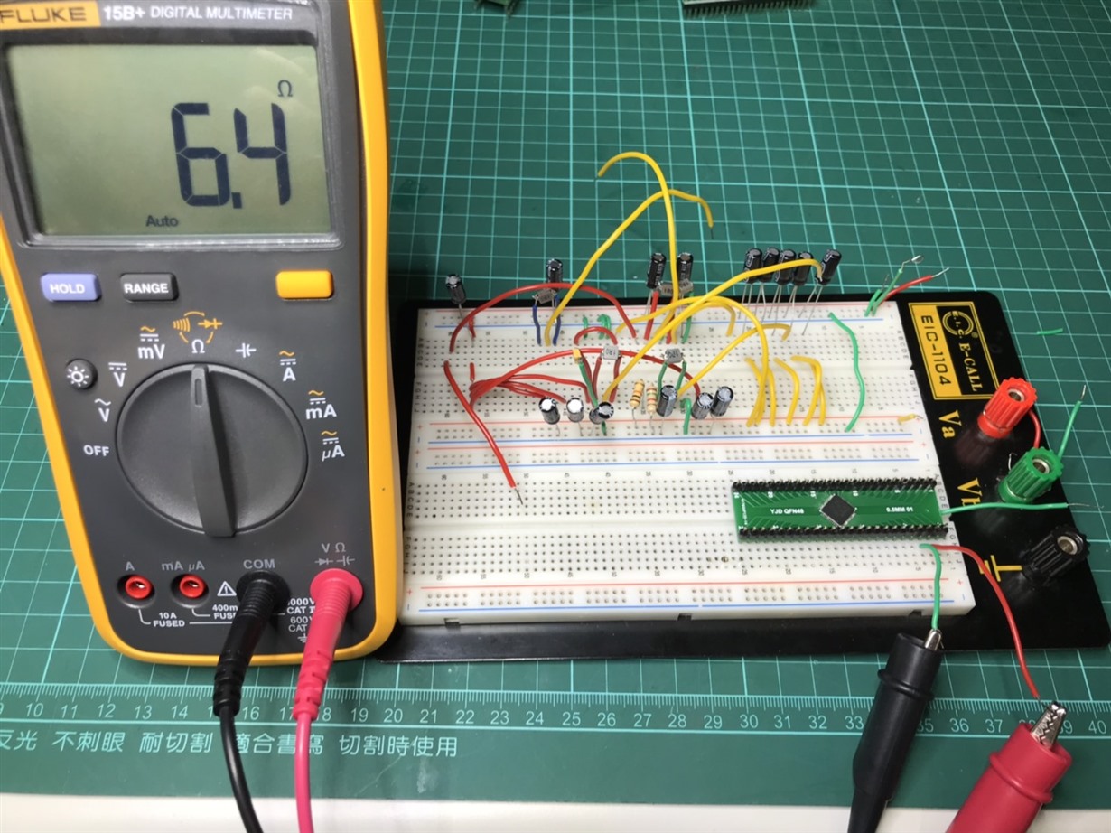
    I soldered the TPS659162 to the PCB and measured each SMPSX_IN and SMPSX_SW point-to-point measurement. They showed an open circuit. Then I connected the peripheral components and gave the voltage to work. I found that the power supply was in current protection mode. At this point, I removed the TPS659162 peripheral components, and once again measured the SMPSX_IN and SMPSX_SW point-to-point and found that they were short-circuited(Conduction).

    As shown, the internal MOSFET appears to be conducting.

    Thanks,

    DAN

  • Dan,

    I recommend you look at some user guides on DCDC convertors. A list of some useful application notes can be found here: www.ti.com/.../slva958

    I especially recommend you look at the article about layout: www.ti.com/.../slyt614.pdf

    Without a good layout, a DCDC converter cannot work properly. Putting a PMIC on a breadboard will not work. The capacitors must be very close to the device to operate correctly. Likely, you are damaging the PMIC because there is so much additional inductance and resistance between your device and the external components.

    I recommend using a PCB, such as our EVM to help your testing: www.ti.com/.../TPS65916EVM

    If you don't want to use our EVM, you can use it as an example for your PCB design.

    Thanks,
    Nastasha
  • Hi Nastasha,

    If I connect SMPSX_IN to 5V, SMPSX_FB is grounded, SMPSX_SW is floating。
    Does this cause damage to the internal MOSFET of the SMPS?

    Thanks,
    Nastasha
  • Dan,

    Yes, this will damage the device. By grounding the feedback (FB) pin, you are shorting the output to ground and preventing the SMPS from regulating correctly. Please follow our guidelines on how to use the device in out datasheet and/or the EVM user guide.

    If you have additional questions, please begin a new thread.

    Thanks,
    Nastasha