This thread has been locked.

If you have a related question, please click the "Ask a related question" button in the top right corner. The newly created question will be automatically linked to this question.

UCC28C42: ACS measurent query

Part Number: UCC28C42

Hello TI,

Seeking your help in understanding the few test parameters test methodology for UCC28C42 PWM controller.

1. ACS (GAIN) of PWM Comparator. As test condition says at Vfb = 0V, vary the Vcs from 0V to 0.9V to measure voltage variation at COMP pin. But COMP output depends on CS input? Also I tried simulating in TINA with datasheet test condition and I don't see any voltage change at COMP pin.

Can you assist me how do I do this?

2. Open Loop Voltage gain for Error amplifier. can you illustrate the  test method for this test with respect block diagram.

Waiting for your reply.
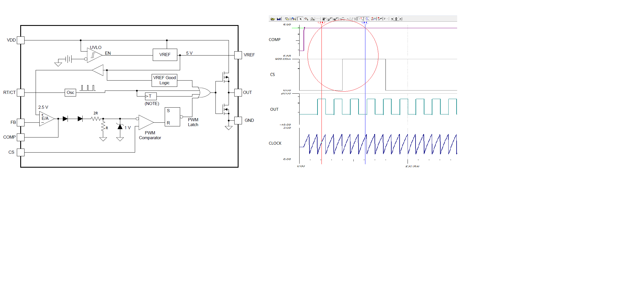
Regards,

Swamy M.

  • Hi Swamy,

    Thank you for your question, and I am working on it.

    Best Regards
    Teng
  • Hi MOGILIKOLLA,

    First, please allow me to correct a point in your question. Gain of PWM Comparator is a wrong expression, since the comparator only outputs high-lever voltage or low-lever voltage by comparing the two input voltage.
    From block diagram, we can see that internal reference voltage of error amplifier is 2.5V, if Vfb is set as 0V, output voltage of error comparator will be saturated, Comp pin Voltage will keep high-level voltage as shown in your simulation result chart. Then it connect to inverting input to PWM comparator and there is a 1V Zener diodes, so the inverting input voltage of PWM comparator is 1V. when Vcs varies from 0 to 0.9V, it always lower than 1V, it does not affect the output of PWM comparator.
    As for the test condition you mentioned, I have not found it, and I think it is a mistake. Could you provide the place where you see it.
    Open-loop voltage gain for Error Amplifier only depends on the Electrical Characteristics of itself. You can directly refer to datasheet of UCC28C42, which shows that type value of Open-loop voltage gain is 90dB.

    Regards,
    Teng

  • Hi Teng,

    Thanks for detailed explanation. Please have a look at attached.

    I am talking about ACS parameter.

    Regards,

    Swamy M.

  • Hi Swamy M.

    Thank you for position.
    I found that maybe you had some misunderstanding of test condition.
    From the datasheet we can see the test condition is:
    The voltage range of Vcs is 0~0.9V, rather than varies from 0 to 0.9V.
    Then Vfb makes a transient jump from current value to 0V, and calculate Acs = △Vcomp/△Vcs during the transient process.
    So we can not say COMP Pin depends on CS input, it should be explained that the voltage variation of Vcomp leads to the voltage variation of Vcs during the transient process.

    Regards,
    Teng
  • Hello Tang,

    Thanks for your clarification.

    I tried the same in TINA in simulation. But I didn't see any voltage change on CS pin.

    I changed FB voltage from 2.7 to 0V, so that COMP will change 0 to 6.5V. Correct me if anything wrong here.

    Regards,

    Swamy M.

  • Hi Swamy M.

    First, change voltage of FB Pin from 2.7 to 0V, voltage of COMP pin is changed from 0 to 6.5V, it is accordant with that I explained before.
    The reason why you couldn't see any voltage change on CS pin is that the CS pin is an input pin, which is used to sense Primary-side current by connecting to current sensing resistor. But your simulation module is just a open-loop test, there is no signal connecting to CS pin.

    Regards,
    Teng