This thread has been locked.

If you have a related question, please click the "Ask a related question" button in the top right corner. The newly created question will be automatically linked to this question.

TPS61030: TPS61030RSAR IC power booster chip

Part Number: TPS61030

Hello fellow engineer, 

I was told I was going to get a call from you guys for the past three days, but then today I got an email directing me to web sight where they suggest I ask my question here instead. That was kind of rude of your company, but okay. 

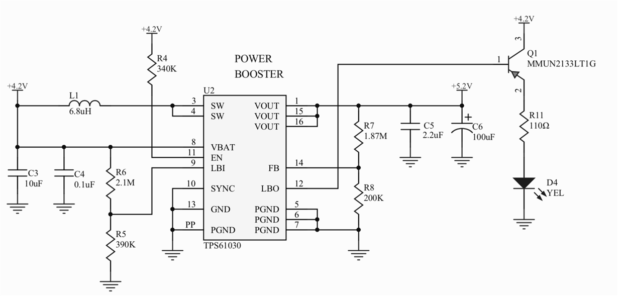
So I'm using your TPS61030 chip in my circuit as shown below, but the circuit was not producing enough amps to run my system. Below is figure of my circuit with your TPS61030 IC chip. 

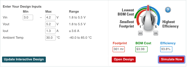
I then found out your web sight has a circuit simulator for this particular chip, that depending on your input values it makes a circuit for you, which is nice. Here is the your websites simulator for reference: https://webench.ti.com/webench5/power/launch_wb.cgi?part=TPS61030&fromdisty=digikey

Then here are my input values for that web sight 

Then this is the circuit it pumped out
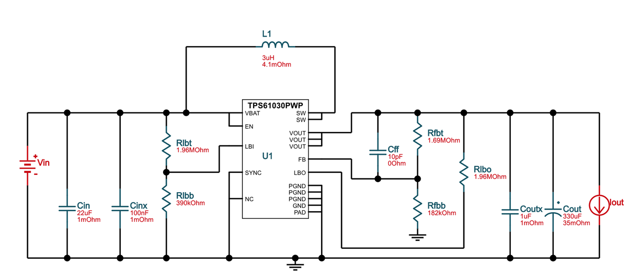
So it looked like to me that all I needed to do was replace a few values of the chips around the TPS61030 IC chip. So I switched out the R4 340K ohm resistor, in my circuit, to a 200K ohm resistor, I also switched in a 330 uF capacitor for C6, and a 3.3uH inductor for L1. 

I then tested this to find out that your TPS61030 IC chip would only produce the amps I needed if given 3.7 V or over. But I needs it to produce up to 1.3 Amps of current with an input voltage as low as 3 V, like I inputed into your online circuit simulator. What is going wrong and how can I fix this? I'm hoping that I can just replace the values of certain chips rather than redoing the schematic on my new PCB. Once this problem is solved I will be able to finish my senior design project at USU and begin manufacture of my product; therefore, buying in bulk from you guys on various parts. Thank you for the support! Please give me a call or email me if you have any questions.

Best,

Kai Gull

kaigull@sbcglobal.net

(630)740-9189

  • Hi Kai,

    Just let you know that our engineers supporting this part will respond soon. Just note that they are in a different time zone and currently they are in weekend.

    Thanks,
    Youhao Xi, Applications Engineering
  • Awesome. I look forward to hearing from them! Thanks for getting back to me so soon. 

  • Hi Kai,

    Could you share your layout? i can check if the issue is not caused by the layout.

    you mentioned the device can't support 1.3A when VIN is lower than 3.7V. so what happen if the VIN=3.6v and IOUT=1.3a. Could you measure the waveform of the input, SW and output?

    i would suggest 6.8uH inductor to reduce the current ripple.
  • Dear Jasper Li,

    Do you mean the PCB schematic layout? There should be three pictures attached to my question, the first one being my PCB schematic layout pertaining to the power booster circuit. The last picture is your web-site's simulated circuit based off the second picture's input. Also notice that I then explain, that I changed the values for some of the chips, around the power booster schematic, which is giving the results I'm sharing with you. 

    Yes it seems that when the DC voltage, Vin, from a 5 Ah, 4.2 V (charged) to 3 V (dead) Li-ion battery, goes below 3.7 V it struggles to give the Vout enough current to run the system. My system requires 1.2 to 1.25 A to function fully. 

    I would ideally like to know what chips values I need to change to enable the power booster IC chip to be able to produce more than enough current to power my system. Does that make sense?

    --

    Kai 

  • Hi Kai,

    the first picture is the schematic, not the PCB layout. I didn't see problem in the schematic, so i want to check the PCB layout. this application note is about how to make a good layout "www.ti.com/.../slva773.pdf"

    The device should support this current from 3V input. so I don't know what is happen in your circuit. that is why I need the VIN, SW, VOUT waveform to debug the circuit. here is a blog about debugging a boost "e2e.ti.com/.../tips-in-debugging-a-boost-converter". I can only make right suggestion after finding the root cause.
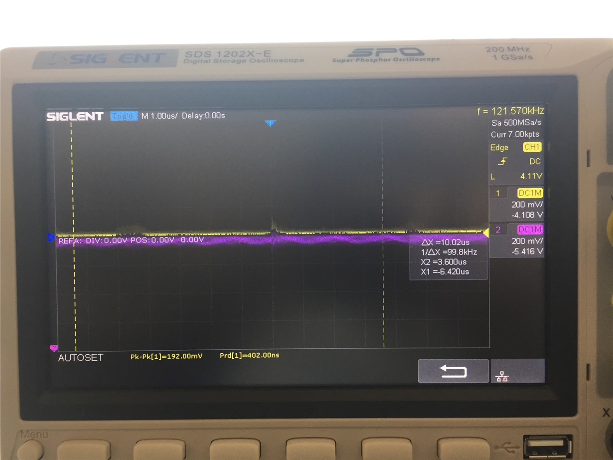
  • Vin (yellow) and Vout (purple) waveforms:

    Looks like for some reason the power booster is outputting 5.416 V DC when it should only be outputting 5.175 DC, which is weird.
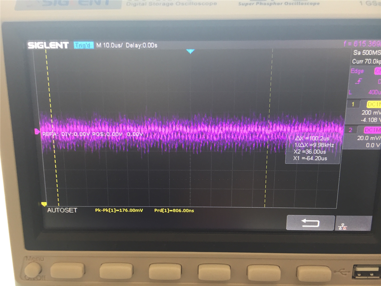
    Below is the SW waveform:
    The layout was created by an expert that has over 50 years experience. I'm a student and my job is designing the schematic, he creates the PCB files from my schematic and designs the layout so I'm sure the layout is correct. I don't have the layout files with me but I can ask him for them, if you really think that is the concern. 
    Best
    Kai
  • So I went into the lab today and looked at the TPS61030 chip under a microscope and it looked like some of the connections may have not been completely soldered correctly. Is it possible that, that may be the problem? That the power booster could still work with only some of the connections soldered, but consequentially not produce over 1 Amp?
  • Hi Kai,
    the switching waveform is not correct. you can find what does the SW waveform look like in my blog "e2e.ti.com/.../tips-in-debugging-a-boost-converter"

    could you try to check the behavior in two other boards?
  • Yes I will assemble another board this week when the parts arrive. 

    Also I want to double check with you that you're sure that, that power booster can support 1.3 A at 5.2 V from 3 V.

    It occurred to me that the amount of input current I need depends on the ratio of output voltage to the input voltage.

    Over the long term, boost conveters are constant-power devices with some loss: to get 1.3A @ 5V out (6.5W), an ideal boost converter would need 1.76A @ 3.7V of input (also 6.5W). No converter is 100% efficient though, and at 90% efficiency you need 1.95A @ 3.7V of input (6.5W + 650mW loss).

    If you drop the input voltage to 3.3V, the current has to rise to about 2.2A. Right? 

    Over the short term, boost converters are constant-current devices whose long-term input and output currents are chopped by PWM, with the PWM duty cycle based on the ratio of the input voltage to the output voltage. 5.2V/3.7V=1.4, so an ideal boost converter's duty cycle would be 1.4:1 or 58% to 42%. The 1.3A long-term average output current is really a series of 1.3/0.42=3.1A bursts at a 42% duty cycle. The input current is also 3.1A chopped by a 58% duty cycle, or 1.8A. That's an ideal ratio though, and taking the 90% efficiency into account raises the input current to about 1.95A, and 1.95A/0.58=3.4A.

    If we drop the input voltage to 3.3V, the ratio becomes 5.2/3.3=1.57, so an ideal converter's duty cycle would be 61% to 39%. The 1.3A output current would become 1.3/0.39=3.33A chopped at a 39% duty cycle, and the input current would be 3.33A chopped at a 61% duty cycle, or 2A. Adjusting for 90% efficiency takes the input current up to 2.2A average, or 3.6A chopped at a 61% duty cycle.

    Even those are only approximations of what happens during one boost cycle though. The instantaneous current rises during the input phase and decays during the output phase, with the instantaneous maximum and minimum depending on the inductor and duty cycle. The TPS61030 seems to stay in the region where the rate of change is nearly linear, but the maximum instantaneous current is still a few hundred milliamps higher than the minimum.

    The 3.4A and 3.6A average values calculated above are only a few hundred milliamps away from the TPS61030's 4A absolute maximum switching current, so the problem may be that the instantaneous peak is hitting that 4A limit. Is that incorrect? I hope I'm wrong and that you're right because that makes things a lot easier. It just costs money and time to assemble another board, both of which I have little of because I'm a mechanical engineering student and it's finals this week. So it would be nice to know that my schematic defiantly correct before I assemble another board. Please let me know what you think. Thanks so much for your patience! 

  • Hi Kail,

    The device can support 5.2V 1.3A from 3V input.
    the output current does change with input voltage, as the device limits its input peak current. please refer to this application note for the calculation. "www.ti.com/.../slva372c.pdf".
    I don't understand how do you get 39% or 42% in the calculation.

    I would suggest you apply or buy an EVM form TI.COM for reference.

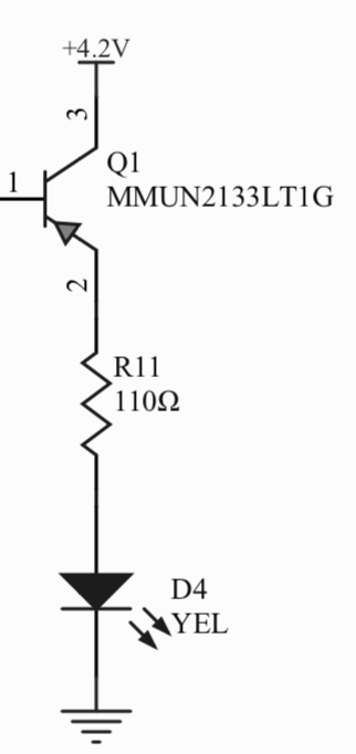
    I don't find issue in the boost converter schematic. one problem is the Q1 for LED circuit. it looks strange. I'm not sure if it is correct.

    before manufacture of your project, it normally requires validation of the solution in several boards. so I don't understand why do you only have one board.

    you mentioned the connection of the IC is not completely correctly. please try to re-solder the IC.

    please also share the image of the layout.
  • Jasper Li,

    Okay that's good to know. Thank you! 

    It looks like the EVM kit is not available... http://www.ti.com/tool/tps61030evm-208 

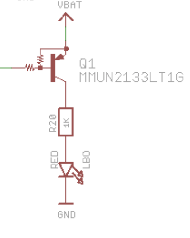
    I got the schematic idea, for Q1 LED circuit, from Adafruit https://learn.adafruit.com/adafruit-powerboost-1000-basic/downloads 

    All the parts are almost here to solder and assemble another board! It sounds like you're saying, that when assembling the board this time, I should use the exact chip values shown in my original schematic? Or should I use a 200 KΩ resistor in place of R4 and a 220 uF capacitor in place of C6? Or other suggestion?

    I'm wondering about the values of the chips because my original schematic reflects the Adafruit power boost 500 basic, which is meant to supply only 500 mA  https://learn.adafruit.com/adafruit-powerboost/downloads 

    That's why I'm wondering if using the Adafruit power boost 1000 basic schematic is a better choice because it's meant to supply 1000 mA, which is closer to what my circuit demands. The only difference between the two Adafruit schematics is a 200 KΩ resistor and two 100 uF capacitors in parallel, hence the 220 uF capacitor. https://learn.adafruit.com/adafruit-powerboost-1000-basic/downloads

    Hopefully that clears things up with my concern about the values of the chips. 

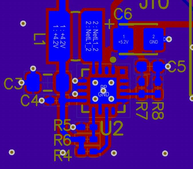
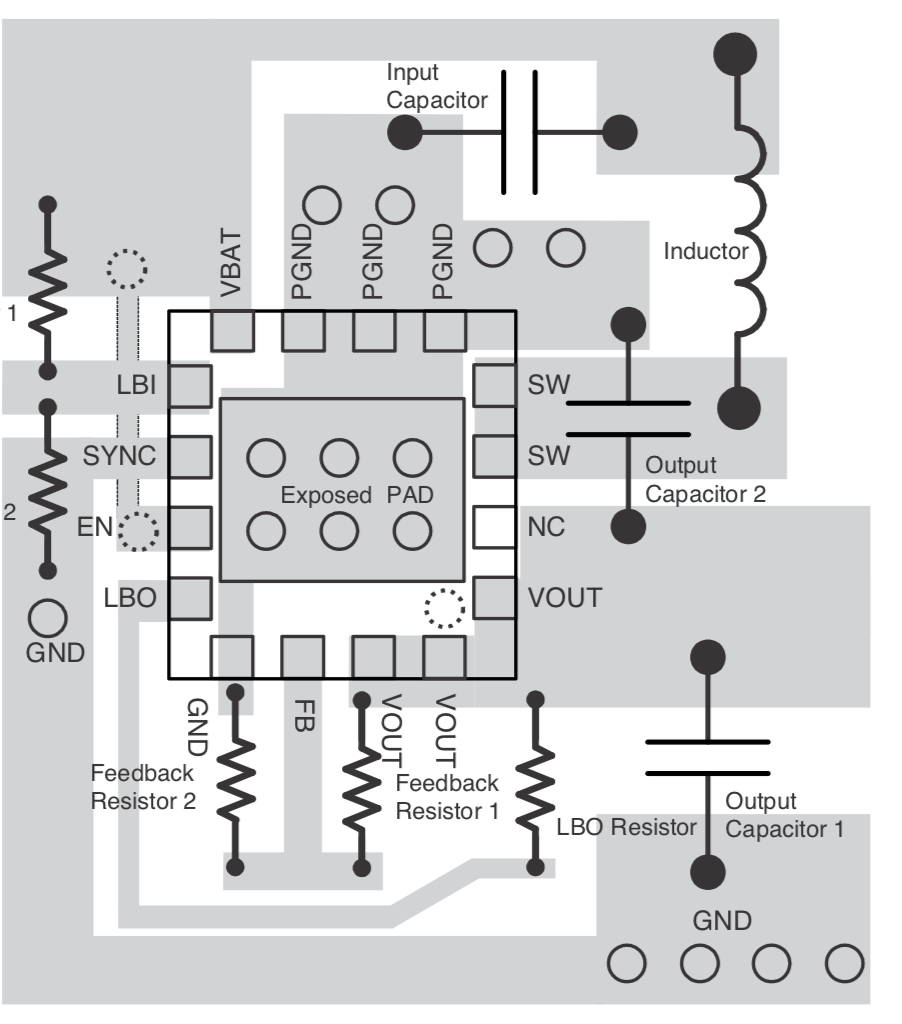
    Also below is a view of the circuit layout you asked for. This is looking at it from the bottom side of the PCB. Is this the layout picture you are looking for?

    Thanks again for helping me out!

    Best regards,

    Kai Gull

  • Jasper Li,

    Okay that's good to know. Thank you! 

    It looks like the EVM kit is not available... http://www.ti.com/tool/tps61030evm-208 

    I got the schematic idea, for Q1 LED circuit, from Adafruit https://learn.adafruit.com/adafruit-powerboost-1000-basic/downloads 

    All the parts are almost here to solder and assemble another board! It sounds like you're saying, that when assembling the board this time, I should use the exact chip values shown in my original schematic? Or should I use a 200 KΩ resistor in place of R4 and a 220 uF capacitor in place of C6? Or other suggestion?

    I'm wondering about the values of the chips because my original schematic reflects the Adafruit power boost 500 basic, which is meant to supply only 500 mA  https://learn.adafruit.com/adafruit-powerboost/downloads 

    That's why I'm wondering if using the Adafruit power boost 1000 basic schematic is a better choice because it's meant to supply 1000 mA, which is closer to what my circuit demands. The only difference between the two Adafruit schematics, is a 200 KΩ resistor and two 100 uF capacitors in parallel, hence the 220 uF capacitor. https://learn.adafruit.com/adafruit-powerboost-1000-basic/downloads

    Hopefully that clears things up with my concern about the values of the chips. 

    Also below is a view of the circuit layout you asked for. This is looking at it from the bottom side of the PCB. Is this the layout picture you are looking for?

    Thanks again for helping me out!

    Best regards,

    Kai Gull

  • Jasper Li,

    Okay that's good to know. Thank you!

    It looks like the EVM kit is not available... www.ti.com/.../tps61030evm-208

    I got the schematic idea, for Q1 LED circuit, from Adafruit learn.adafruit.com/.../downloads

    All the parts are almost here to solder and assemble another board! It sounds like you're saying, that when assembling the board this time, I should use the exact chip values shown in my original schematic? Or should I use a 200 KΩ resistor in place of R4 and a 220 uF capacitor in place of C6? Or other suggestion?

    I'm wondering about the values of the chips because my original schematic reflects the Adafruit power boost 500 basic, which is meant to supply only 500 mA learn.adafruit.com/.../downloads

    That's why I'm wondering if using the Adafruit power boost 1000 basic schematic is a better choice because it's meant to supply 1000 mA, which is closer to what my circuit demands. The only difference between the two Adafruit schematics, is a 200 KΩ resistor and two 100 uF capacitors in parallel, hence the 220 uF capacitor. learn.adafruit.com/.../downloads

    Hopefully that clears things up with my concern about the values of the chips.

    Also below is a view of the circuit layout you asked for. This is looking at it from the bottom side of the PCB. Is this the layout picture you are looking for?

    Thanks again for helping me out!

    Best regards,

    Kai Gull
  • so sorry for three exact same replies! your web sight was glitching!
  • Hi Kai,
    you can apply TPS61030EVM-029, which is for QFN package, same package as in your system board.

    the Q1 circuit in the link is not the same as in your schematic.
    you can use the components as in your schematic. could you share the part number of the 6.8uH inductor and 100uF C6?
    changing R4 to 200K don't help the issue. for the C6, if the spec of the capacitor is closed to the one used in the EVM, you don't need to change it to 220uF.

    yes, the image is what I was looking for. I think the pin 5~7 should be connected to the thermal pad directly. but it may be not the root cause of the behavior you observed.
  • Okay here are all the chips that you may be interested in looking at:

    Q1 = MMUN2133LT1G = www.digikey.com/.../2705149

    6.8 uH inductor = VLS5045EX-6R8M = www.digikey.com/.../en

    100 uF capacitor C6 = TPSB107M006R0250 = www.digikey.com/.../1888189

    220 uF capacitor C6 alternative = TLJT227M006R2000 = www.digikey.com/.../2197011

    R4 200K resistor = RC0402JR-07200KL = www.digikey.com/.../729387

    You're right that the schematic for Q1 is slightly different from the schematic I have, in that the arrow should be going from 3 to 1 rather than from 2 to 1. I actually didn't notice that until you just pointed it out now thank you! I wonder if, that even though the arrow shows a different direction in the schematic, if in reality the MMUN2133LT1G (being the same chip that they use) acts in the correct way because there is only one way to install it on the board. What do you think?

    The chips will arrive tomorrow night, so Friday morning I will solder another board with the chips values that reflect my original schematic. Thanks again for everything!
  • Hi Kai,

    The inductor is good.
    the ESR of the 220uF is too large, 2ohm, so it can't be used.
    the ESR of the 100uF is also not small, please has two of them in parallel. normally i would suggest 50m level ESR.

    I don't fully understand your meaning about the Q1 circuit. but i would suggest you copy the circuit in the Adafruit. i'm not sure if the current circuit can work.
  • Hi Kai,
    I haven’t heard back from you, I’m assuming you were able to resolve your issue. If not, just post a reply below.
  • Dear Jasper Li,

    Sorry for the late response! It's been Christmas break and the campus lab is closed, so I had to buy all the tools and set up lab at home. I'll let you know when it's working when it does (:

    So to confirm your instructions:

    1. Your saying I should find a 100 uF capacitor with an ESR of 50 mOhm, rather than 250 mOhm? Also that I should put two of them in parallel to give a total capacitance of 200 uF? 
      1. Do you recommend to put two of these capacitors in parallel? https://www.digikey.com/product-detail/en/avx-corporation/TCJY107M016R0050/478-9490-1-ND/5001702
      2. Could I instead use this single 220 uF and save over a dollar in cost per board? https://www.digikey.com/product-detail/en/avx-corporation/TCJY227M006R0050/478-9503-1-ND/5001715
      3. Or do you know of a capacitor you could recommend to me?

    2. For the Q1 circuit I was clarifying that you noticed that my Q1 transistor is backwards, compared to the Adafruit schematic, as shown below. Is that what you meant?  
      1. My schematic                                 and Adafruit's schematic 
      2. Are you saying that I should design that part of the schematic a completely different way or just correct it to the way Adafruit has it?
    3. I was able to solder my PCB again using the original chip values in the original schematic, as shown below, to double check if it was a soldering issue.
      1. The results where the exact same as before, meaning it was not able to power the entire system when the voltage dropped below 4 V; therefore it was not a soldering issue. Again I want to clarify that changing the capacitor to the 220 uF with the ESR of 2 Ohm (https://www.digikey.com/product-detail/en/avx-corporation/TLJT227M006R2000/478-5989-1-ND/2197011) did allow the system to fully run given over 3.7 V which is better than 4 V.

    It seems you are telling me the problem is that the resistance in the capacitor was too large?If you are sure about this I will remanufacture the PCBs with a corrected footprint to fit the new capacitors and also will correct the Q1 circuit. What do you think? 

    Best,

    Kai

  • Hi Kai,
    1. you can use one 220uF capacitor for C6.
    2. You should follow the circuit in Adafruit.
    3. the 2ohm ESR may work for stable application. but you would observe large ripple in load transient condition. I still suggest 50mOHM~100mOHM ESR capacitor.
  • Again the original circuit, now soldered twice, behaves the exact same meaning it is not able to support 1.3 A at 3 V. The voltage has to be at or above 4 V in order for it to support 1.3 A. So I don't know what you mean by "the 2ohm ESR may work for stable application."

    Is the reason the circuit can't support 1.3 A as low as 3 V is because the C6 capacitor had a ESR of 2 Ohm rather than 50~100 mOhm? I will order that capacitor now to test it in my circuit, two days shipping. 

    Kai

  • Hi Kai,
    OK, i misunderstood your meaning.

    please change the capacitor.
  • Before you mentioned the below about the PCB layout:

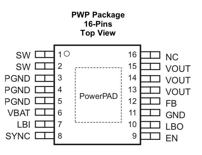
    So you're saying pins five though seven should be connected to the thermal pad? The below shows pins five through seven on the IC chip data sheet.

    When the data sheet does not show those pins connected the the thermal pad directly as shown below. I'm confused could you please clarify.

    Also concerning the original topic before why did you change your mind about the C6 capacitor? Originally you said my schematic looked good with the single 100 uF capacitor, but now you changed your mind saying I need two 100 uF capacitors in parallel or a single 220uF capacitor. Why did you not mention this in the beginning? 

    Is there a way I could call and talk over the phone with you or another engineer that specializes in this IC chip?

    Kai 

  • Hi Kai,
    I am not sure if you are aware that the TPS61030 has two package, PWP and RSA. the first image you share is PWP and the layout image is RSA package. the pins definition of the two packages are different.

    The capacitance of the C6, 100uF or 220uF, should be not the root cause of the behavior you observe from my experience. so I didn't mention output capacitor at the beginning. I had been working for switching power for more than 20 years.
    as the datasheet suggests 220uF capacitor, I suggest 220uF to avoid any confuse. I apologize for no making it clear from the beginning.
  • Hi Kai,
    any update after the modification?
  • After replacing the C6 capacitor the voltage showed to be 3.5 V output from a 4.2 V input, when it should be 5.175. I then removed the Q1 transistor and that did not effective the voltage. I'm still trying to diagnose why this is happening now.  

  • Hi Kail,
    please don't add large loading before the device finished startup. let me know if there is further finding.