This thread has been locked.

If you have a related question, please click the "Ask a related question" button in the top right corner. The newly created question will be automatically linked to this question.

UCC27533: The interface circuit design between UCC2753X and CPLD, when the UCC2753X GND pin is negative.

Part Number: UCC27533

I am designing a gate driver for sic mosfet module using the ucc2753x. The sic mosfet is powered by a positive and a negative bias. That means the GND pin must be negative, however all the input signals of ucc2753x are reference to this node.

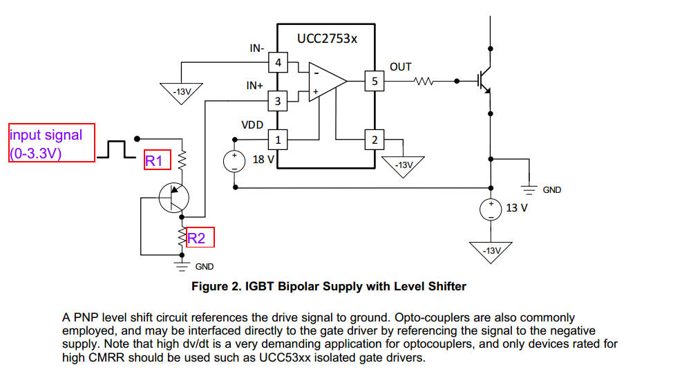
A PNP level shift circuit references the drive signal to ground is proposed in document SLUA169A, which is shown in the figure. 2.

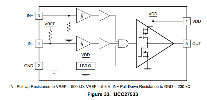
As shown in Figure2, when IN- is -13V. if IN+ voltage is higher than -11.8V (-13v+1.8v), the OUT is 18V, if the IN+voltage is lower than than -12.2V (-13v+0.8v), the OUT is -13V. the selection of 1.8V and 0.8V is based on the datasheet of ucc2753x, as shown in the following figure.

The IN+ is pulled down to -13V with a 230kΩ resistor as shown in Figure 33. if the input signal is 0V. the R2 can be calculated with formula R2>230kΩ*(12.2/0.8)=3.5MΩ


Has anyone evaluated the speed of the PNP level shift circuit, as shown in Figure 2?

if the speed is ns level, can anyone recommend a high speed pnp transistor?

If the speed is low, Is there any other level shift circuit from TTL to negative negative voltage that can improve the speed between the input signal signal and the ucc2753x?


  • Hi CHENGFEI,

    Thanks for reaching out to the High Power Drivers team, my name is Mamadou Diallo, I am the AE supporting this device.

    Prop delay of the level-shifter is dependent on couple of factors including choice of resistors. High resistors values will reduce current through the level shifter and degrade your prop delay significantly whereas low resistors values will increase current through the level shifter leading to increase in power dissipation (while keeping in mind the current capability from the MCU) within the level shifter.

    On your equation above, you mentioned R2 > 230kOhms*(12.2V/0.8V). In theory, you're correct but that if you choose a 3.5MOhms of resistance in your circuit, your prop delay will be significantly compromised. In order to achieve good timing characteristics, high current is required through the transistor which means smaller resistor values.

    First, I would advise as first step to know the current capability of your MCU and depending on that, size the resistors (typically <300-Ohms) accordingly to allow enough current through the transistor. Generally speaking, transistors with good BW and current ratings should work as long as you size those resistors appropriately.

    I am looking further into this circuit and will get back to you.

    Thanks.

    Regards,

    -Mamadou
  • Hi Chengfei,

    Thanks for your patience,

    I will get back to you by End of business day tomorrow (Dallas time).

    Thanks.

    Regards,

    -Mamadou
  • Hi Chengfei,

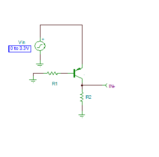
    For the speed requirement of your application, consider the slightly modified level-shifter to help enhance prop delay while being aware of potential trade-off of power dissipation at the junction of the transistor. By relocating R1 from emitter to base, you increase the collector current and reduce prop delay introduced by the the level-shifter.

    Again, you have to bemindful of the power dissipation introduced by the increase in collector current. When choosing your transistors, you want to make sure it is capable of withstanding the power dissipation at your desired speed. You can tune R2 to control this power dissipation and prop delay however values above 300-400Ohms would significantly increase prop delay while reducing current through pnp transistor.

    If this helped address your inquiry, please press the green button or let us know if have further questions.

    Thanks.

    Regards,

    -Mamadou

  • Hi Mamadou!
    Thanks for your answer,
    I have also simulated the PNP shift circuit, if R2 is above 3.5 MΩ, the delay is too long!
    The main problem is that the high speed interface circuit design between the MCU and UCC2753X.
    If the ucc2753x is negative bias with -13V as shown in Figure2, all the input signal is referencd the -13V, that means the resistance R2 must >3.5MΩ, so the pnp level shift circuit is unavailable because the long delay!
    is there any other level shift scheme can solve the problem?

    Thanks
    Regards,
    Chengfei
  • Hi Chengfei,

    Thanks for the follow-up.

    Why exactly must R2 be > 3.5MOhms? From your previous post, your calculation of R2 is "R2>230kΩ*(12.2/0.8)=3.5MΩ". What is your reasoning for the ratio between 12V and 0.8V?
    The proposed level-shifter is referenced to controller ground NOT the -13V. The R2 value is dependent on the current through the transistor and should be calculated based on the current through R2 (collector current) and the voltage across R2.

    Thanks.

    Regards,

    -Mamadou

  • Hi Mamadou!

    Thanks for your answer,
    May be the meaning I expressed is not clear.
    The ucc27533 ground is -13V, all the input signal is referenced to -13V.
    If you want to turn off the igbt or mosfet, the IN+ signal must < (-13+0.8)=-12.2V.
    If you want to turn on the igbt or mosfet, the IN+ signal must > (-13+1.8)=-11.2V.
    The IN+ PULL Down resistance to -13V is 230KΩ。
    if the emitter of pnp transistor is 0V, the current will throuth R2 and 230KΩ from GND(0V) to -13V.
    if the IN+ signal is -12.2V, the R2 is 3.5MΩ.
    so if the IN+ signal <-12.2V, R2 must be > 3.5MΩ.
    Thanks.

    Regards,

    -Chengfei
  • Hi Chengfei,

    Thanks for the response.

    Where I am not clear is your calculation of R2? I agree IN+ voltage levels  to turn-on/off IGBT/MOSFET.

    Are you saying that R2 must be 3.5MOhms to prevent current from flowing from 0V through R2 and 230kOhms to -13V? Is my understanding of your point correct?

    I have attached my simulations schematic along with transient results where I reference both the level-shifter signal and the driver's input to -13V with example resistors values.

    In this case, I use two separate resistors R2 and R4 to help share power dissipation across pnp transistor and as you see in simulation results, R2 is set 650Ohms but doesn't need to be >3.5MOhms when IN+  <-12.2V

    When the emitter of the pnp transistor is 0V, current through AM2 is negligible and should not be a problem.

    Values chosen are example values and should be used as guidelines for the designs only. These values may be adjusted to meet the design requirements.

    Level shifter and UCC27531 negative turn-off bias.zip

    Please let me know if you have further questions or press the green button if this resolved your inquiry.

    Thanks.

  • Hi Mamadou!

    Very Thanks for your answer,
    If the R2 is connected to the -13V, all the problem will be solved.
    I was confused by the Fig.2 in document SLUA169A, because the R2 is connected to the 0V and the ucc27533 GND is -13V.
    Thanks.

    Regards,
  • Hi Chengfei,

    Sorry for the confusion, it is a mistake on our part.
    We will fix it during the next revision iteration.

    Please let us know if you have further questions.

    Thanks.

    Regards,

    -Mamadou