This thread has been locked.

If you have a related question, please click the "Ask a related question" button in the top right corner. The newly created question will be automatically linked to this question.

TPS74901: TPS74901 support 3A application

Part Number: TPS74901
Other Parts Discussed in Thread: TPS74801

Dear Sir,

Customer design TPS74801 for previous projects but the requirement increase to 3A. Could TPS74901 support 3A application?

TPS74901 is same package as TPS74801. Is there any difference between these two parts besides OCP?

Andy Lin

  • Hi Andy,

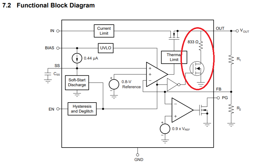
    Yes, the TPS74901 can support up to 3 A output current. In addition to different current limits, the two devices have slightly different thermal performance and dropout voltage specs. The TPS74901 also does not have the output discharge feature found in the TPS74801:

    Thanks,

    Gerard

  • Hi, Gerard,

    TPS74901 has higher thermal resistance. In addition the power loss is same as TPS74801 if Vin to Vout voltage gap is larger than Vdrop. I still can't understand why TPS74901 can handle higher current than TPS74801 in same package.
    Or this package could accept same power dissipation but only current limit is different?

    Andy
  • Hi Andy,

    The maximum output current is determined by the design of the internal pass transistor. The TPS74901 has a larger pass transistor which allows it to supply more output current. This pass transistor is not so much larger that it requires a different package, so both devices are available in the RGW and DRC packages.

    You are correct in thinking that, if the same PCB is used, the maximum allowable power dissipation for these two devices will be the same due to the similar thermal resistance specs. If your application requires 3 A output current, the input voltage may need to be adjusted to ensure that the junction temperature of the device does not exceed 125 C.

    Pd,max = (Vin,max - Vout) * Iout = (Tj,max - Ta)/Rja

    Where
    Vin,max is the maximum allowable input voltage
    Vout is the output voltage required by the load
    Iout is the output current required by the load
    Tj,max is the maximum recommended junction temperature of the LDO, 125 C
    Ta is the operating ambient temperature
    Rja is the junction to ambient thermal resistance

    Keep in mind the Rja is heavily dependent on the PCB layout. If a different PCB is used, the layout can be optimized to reduce Rja by up to 50% by maximizing the amount of copper and thermal vias around the LDO. Reducing Rja will increase the maximum allowable power dissipation.

    Thanks,
    Gerard