This thread has been locked.

If you have a related question, please click the "Ask a related question" button in the top right corner. The newly created question will be automatically linked to this question.

UCC27712: Ringing found in the gate signals generated by ucc27712dr for driving H-bridge for ac generation.

Expert 1140 points
Part Number: UCC27712

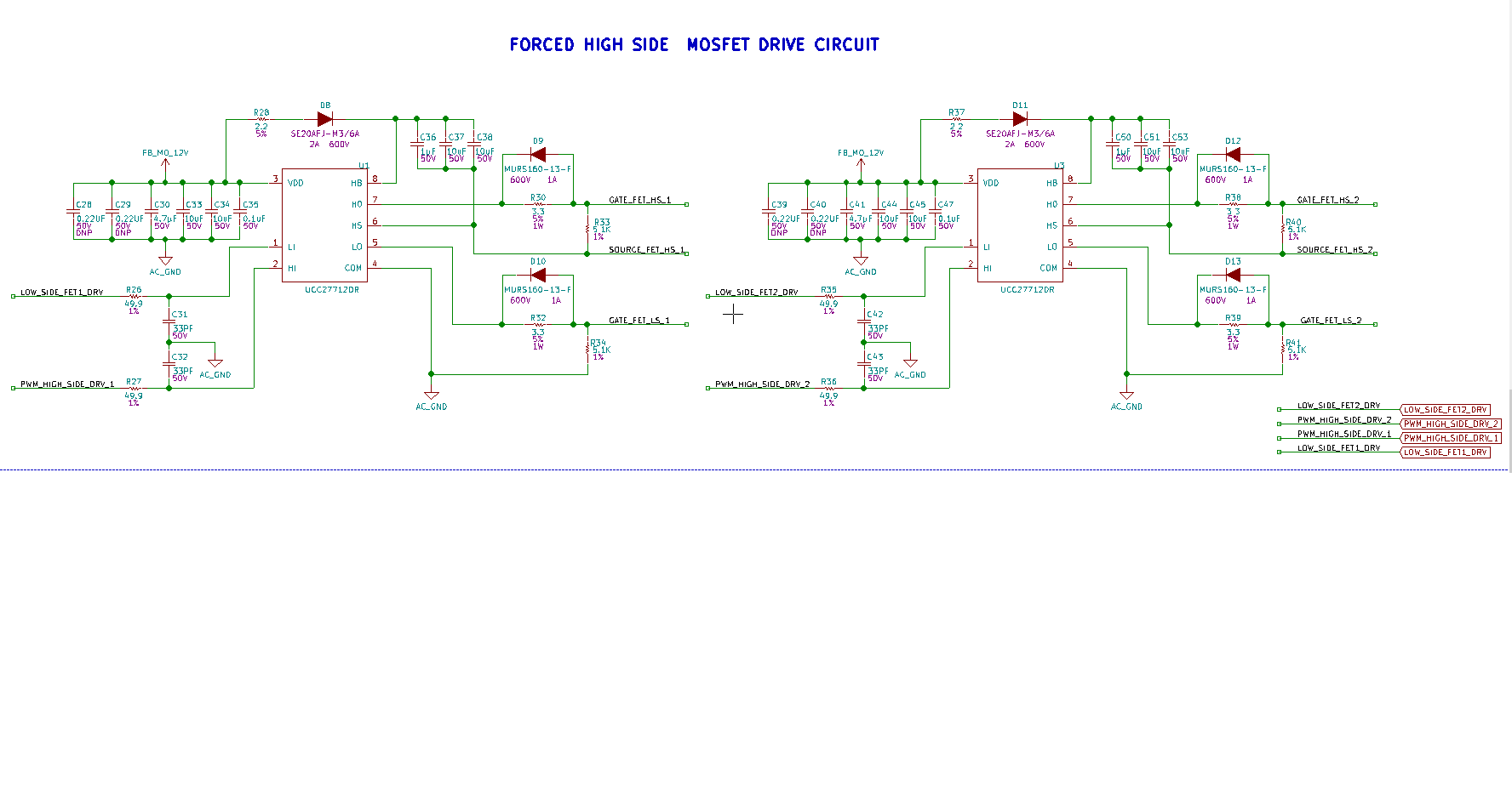
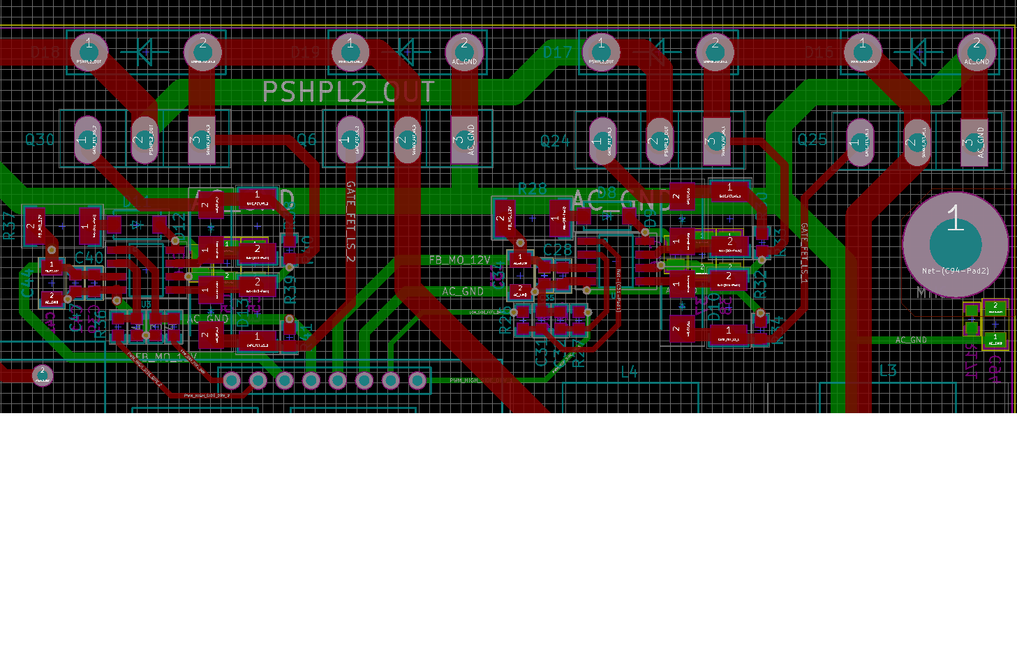
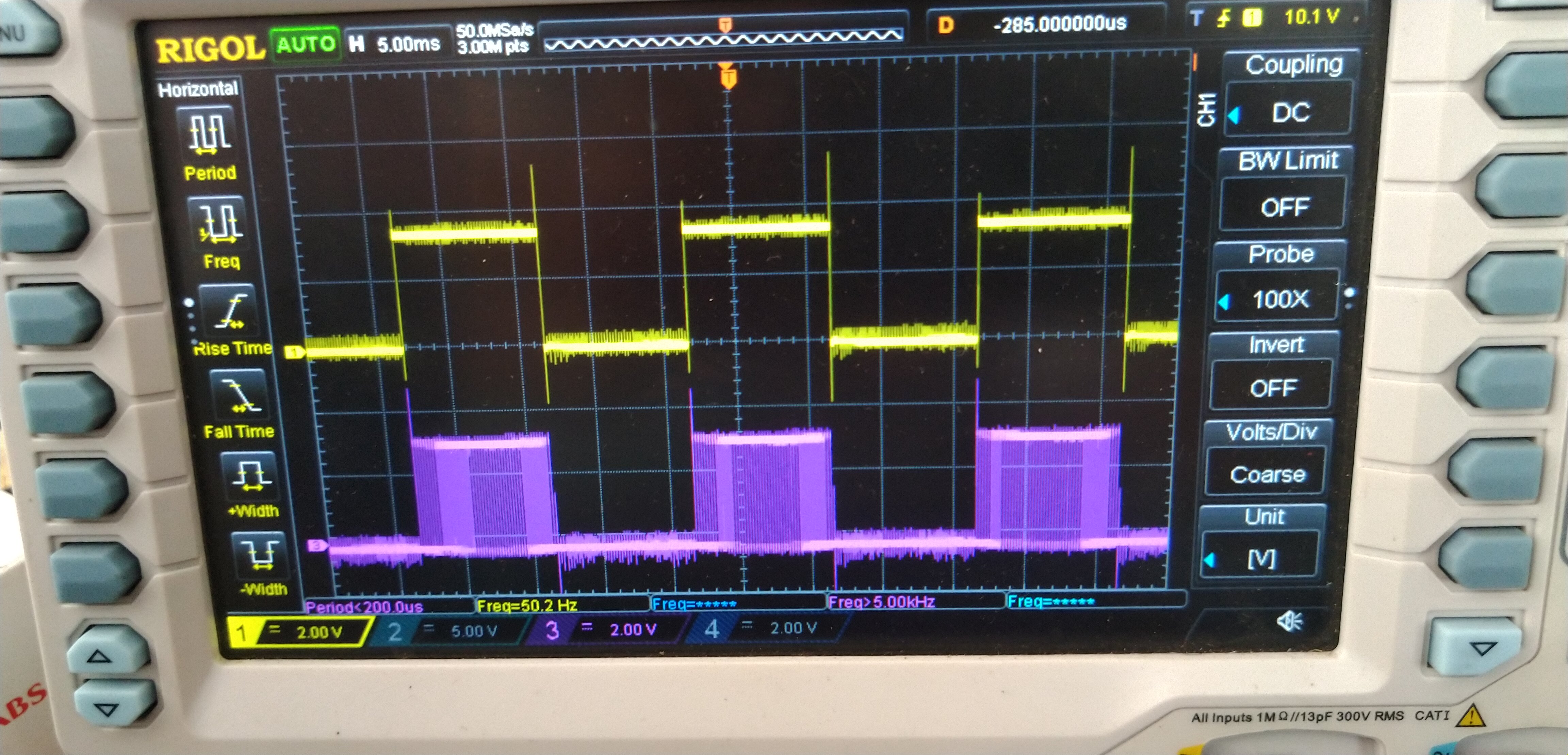
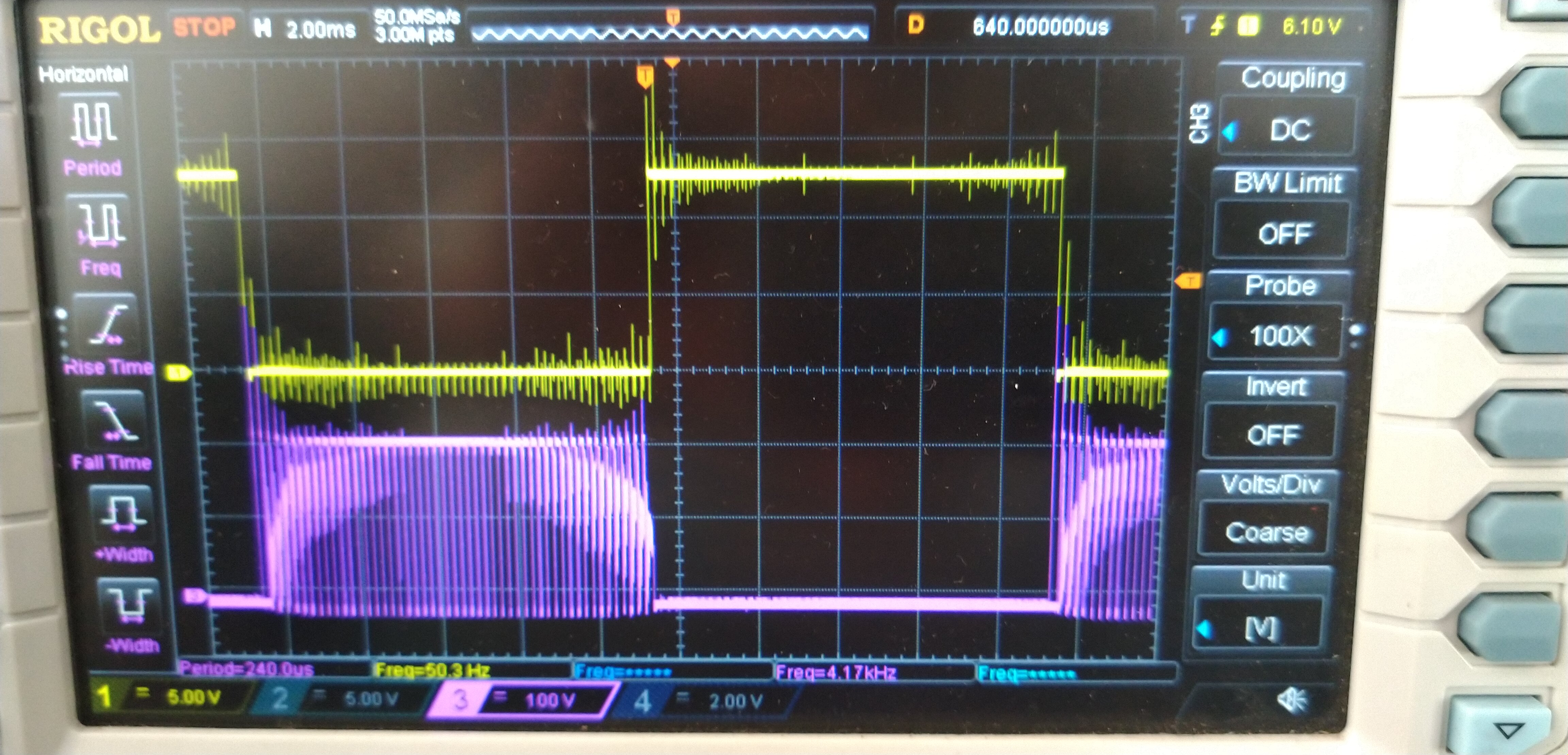
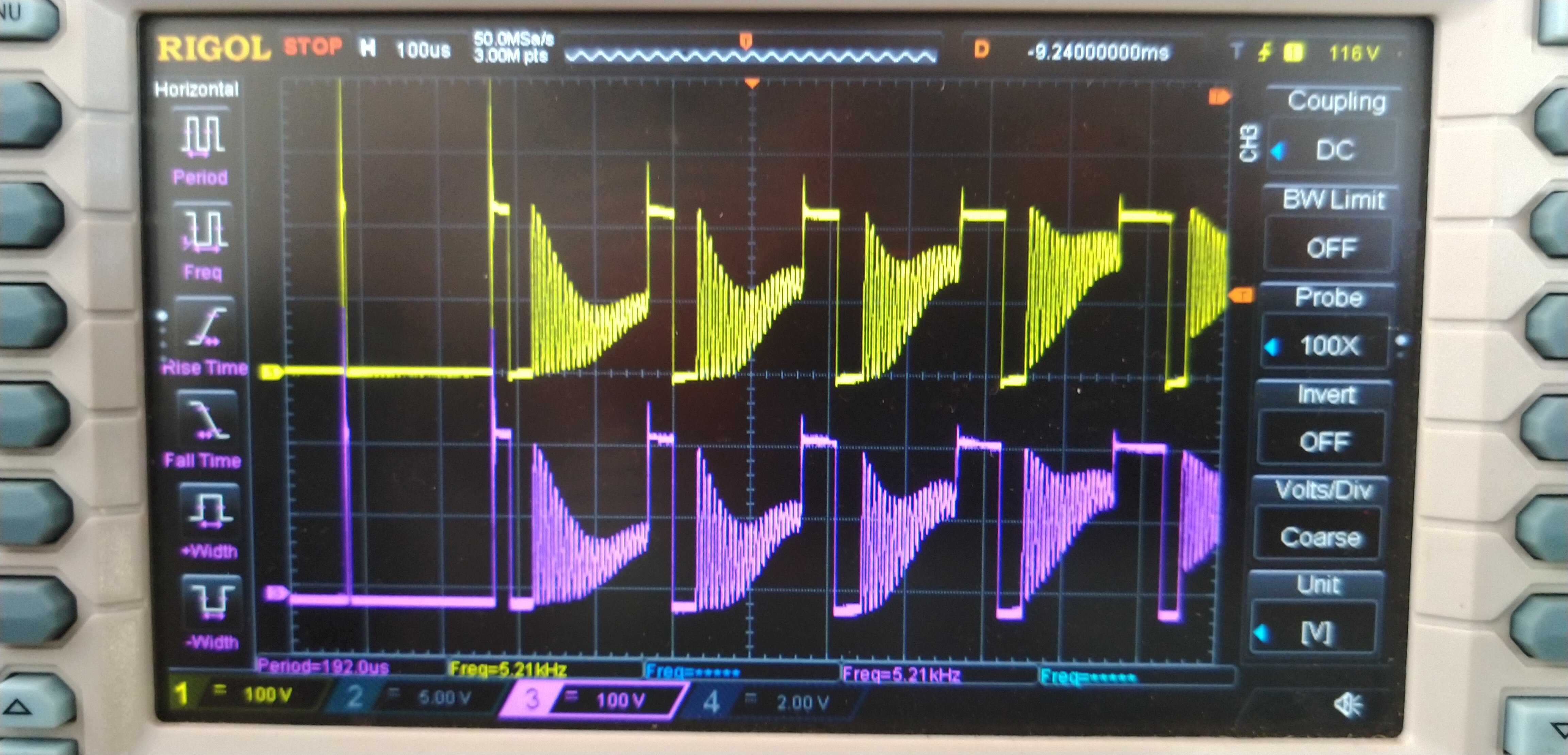
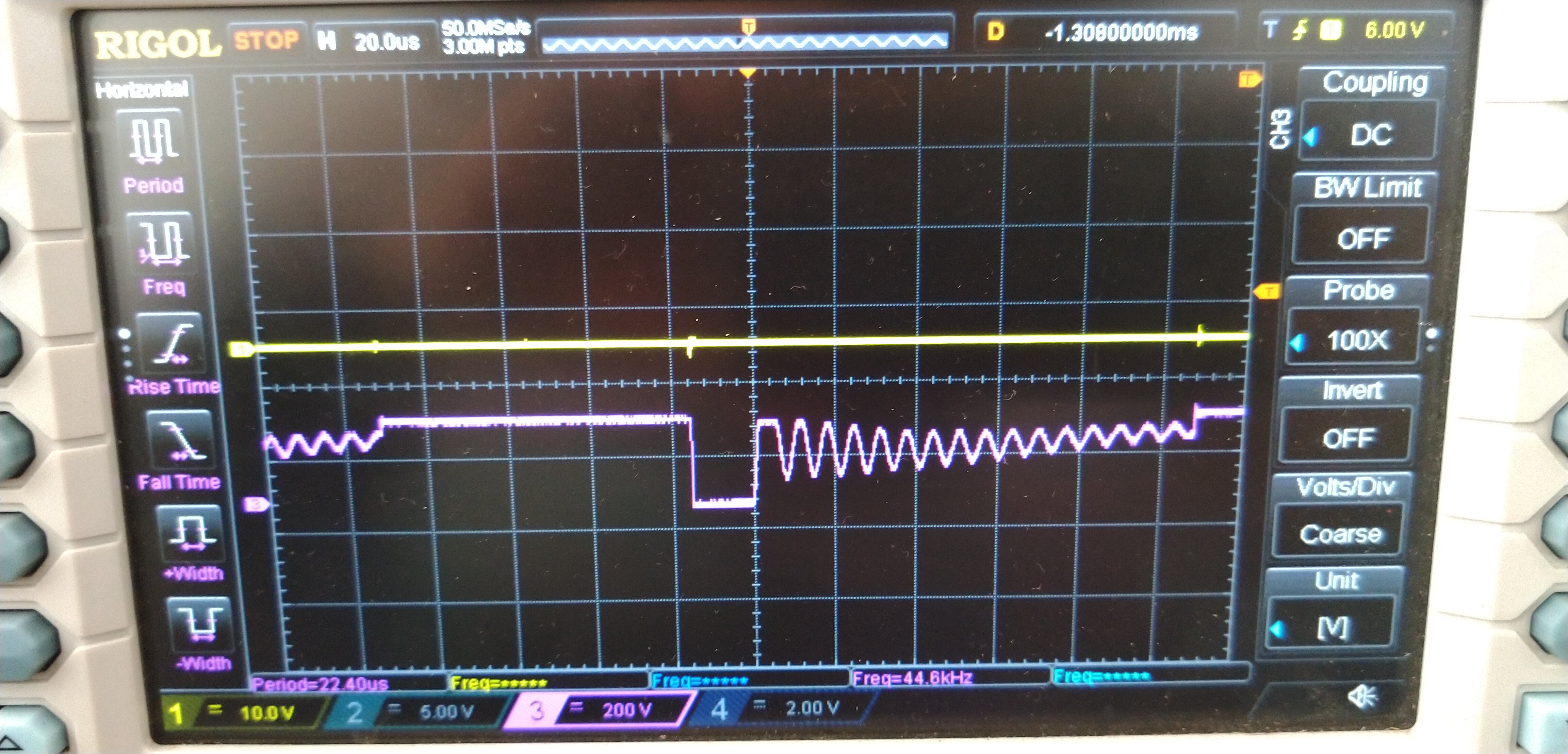
Hai i am designing a 1.65kw solar inverter.i have h-bridge in the output side for 50 Hz ac generation.i am using IGBT STGW20NC60VD AND ARE DRIVEN BY UCC27712DR for ac generation.I have applied spwm with 90 percent duty cycle in the high side and simply square pulses on the low side for ac generation.I found the ringing and peaks as shown in the image in the gate signal which are causing the mosfets to be too hot when high loads are applied at the end of the h-bridge.What could be the possible reason behind this issue?

The image shows signals ,when the gates of the IGBT were probed.

  • Hi Amal,

    Sorry you are having issues with your design.

    My colleague will investigate and get back with you on Monday, Dallas time.
  • Hi,
    Hope i would get the support fast as the project is in a crucial stage.
  • Hello Amal,
    Thank you for the interest in the UCC27712. I am an applications engineer supporting this device and will work to resolve your concerns.
    I have some questions about your application, and requests for additional information and waveforms.

    Can you tell us the switching frequency of the half bridge in your application? The plot looks like ~4us for the period which is 250kHz, this seems very high for IGBT's, please confirm.
    I see the bootstrap capacitance is fairly high at 21uF, which may be needed if there is very low switching frequency. The boot capacitance and VDD capacitance should be reviewed once the frequency is known. We typically recommend a VDD capacitance of 10x the boot capacitance, and the schematic shows ~24.7uF for VDD capacitance and 21uF for the bootstrap (HB-HS) capacitance.

    The waveform shown looks like it must be the HO to ground signal, based on the voltage scale. The high side gate drive is the HO-HS voltage. It is not clear if this ringing is occurring on the HO signal or the HS signal to ground.
    Can you record the scope plot of the HO-HS signal with a differential probe, HS signal to ground, and LO signal to ground?
    Show the same time scale you have, and also zoom in on 1 or 2 switching cycles to see the detail of any ringing and rise/fall times.

    Ringing on the Vgs waveforms is very dependent on the board layout regarding the trace lengths of the driver to IGBT gate, and emitter to driver ground reference. The parasitic inductance of the traces and parasitic capacitance of the power device creates a high Q resonant circuit. I see the gate resistance is a fairly low value at 3.3 Ohms. Higher gate resistance will help lower the Q of the gate drive loop which can reduce the ringing. Although it is not clear how much ringing exists on the HO-HS based on the scope plot attached.

    Regards,
    Richard Herring
  • Hi Amal,

    It's been a while since we've heard from you, so we must assume you've resolved your issue.

    If possible, please post how it was resolved for others to learn from it.

    If your issue isn't resolved, let us know, and we will work with you to resolve it.
  • Hai,

    sorry for late Response,we were having holidays till yesterday.

    The switching frequency of half Bridge is 5KHz.Yaa its true that the VDD caps is not 10x the bootstrap.Should i decrease the bootstrap cap and increase the VDD caps.Or Should i change them?

    The following are the HS AND HO SIGNALS probed with respect to ground.

    Zoomed image of HS AND HO are also attached.Please see the Image of Ho probed with respect to ground.I have also attached the Input waveform to the gate driver driving a half cycle.

    Please note that SPWM is given to high side and square pulses to low side fets.

    i have also attached the routing scheme implemented on my board.please comment on same.

  • Hello Amal,

    Thank you for the details on the operation, scope plots and layout.

    First I want to review the bootstrap capacitor and VDD capacitor values based on the operating frequency and IGBT part number. The value selection guidelines can be found in the datasheet section 8.2. http://www.ti.com/lit/ds/symlink/ucc27712.pdf

    First determine Q total based on device Qg and HB Iq. Since there is a 5.1K Ohm gate to source resistor I will add this current to the Iq. Current from 5.1k resistor: Vdd-Vf/Rgs, 11.3V/5.1kOhm= 2.2mA. This value of Rgs and low frequency will discharge the HB cap noticeably and require larger value.

    Qtotal=Qg +( Iqbs+IRgs)/Fsw, Qtotal= 100nC + (2.2mA + 65uA)/5kHz=553nC. You can see the Rgs current dominates the required charge since the device is 100nC Qg.

    Cboot=Qtotal/deltaVboot=553nC/0.5V=1.1uF

    I would suggest having the Cboot at 1uF to 2.2uF, maybe change the R33 to 10 k Ohms for more margin.

    With Cboot at 1 to 2.2uF, the existing Vdd capacitance of ~24.7uF meets the recommendation of CVDD being 10x the Cboot value.

    On the scope plots second to bottom zoomed in . The CH1 high pulse appears to be ~10V higher than the channel 3 switch node. The remaining waveform appears to be the same which ideally HO will be the same as HS for 0V differential. The very last plot it is not clear of this condition, or trace signals can you explain the last trace signals, and if this is expected operation?

    On the layout plots: Most component placement and trace length looks good. I have a couple of comments. The trace to the LI input looks very close to LO output and HS/HO output. There may be some noise coupling from the high voltage and dV/dt traces to the LI input. Move HI and LI traces as far away from driver outputs as possible. It is not clear where the driver ground reference path to the low side power device emitter connection is routed. Make sure the driver current path length to the gate and from the emitter back to driver ground is not long.

    Since you are driving IGBT, have you tested using higher drive voltage such as 15V to see if this improves the operation?

    If you have more questions or concerns please reply to this post. If we resolved the concerns please confirm on the thread.

    Regards,

    Richard Herring

  • Hai,
    Thanks a lot for your support . Presently we are testing on with the values suggested .Actually my system is destined to drive voltages at range of 300v or more to generate AC with rated rms of 230v.The waveforms you saw were taken at a DC voltage of 200v. Actually I happen to poke more on this mainly because I found unusual temp rise on the high side IGBTS leading me to doubt the gate signals. Actually my major doubt is should I probe my high side signals wrt to source of the IGBTS or ground of the input.I found a clean waveform wrt to source and ringing waveform as in image wrt to common gnd.
  • Hello Amal,
    The meaningful signals to examine are the gate drive signals with respect to the IGBT emitter, especially on the high side drive since that drive signal is referenced to the power train switch node. The ringing of the high side drive with respect to ground, could be the ringing that is on the power train switch node, and still could represent a 0V potential from the high side gate drive and HS pin of the high side driver.

    Let us know if this addresses your questions, or you can ask for additional information on this post.

    Regards,
    Richard Herring