This thread has been locked.

If you have a related question, please click the "Ask a related question" button in the top right corner. The newly created question will be automatically linked to this question.

TPS62260: different PFM waveform - different output voltage ripple

Part Number: TPS62260

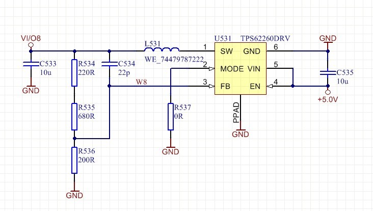
Hello, I use the DC / DC converter TPS62260DRV on several devices. On a device 8 such converters are installed. On some modules (not all) it happens, then one or two of the 8 converters behave differently than the others. But that's not always the case in the same position of the LP. In principle, the converter works almost correctly, it comes out the voltage, which is adjusted by means of the feedback resistors. However, the ripple is different than the other DC / DC converters. The converter with higher ripple has a distinctly different behavior on the SW pin. I first swapped the passive components from a working one to a nonfunctioning one. There was no change. The faulty converter continued to have the higher ripple. Then I swapped the ICs. With the exchange also the mistake went along. So it must have something to do with the DC / DC converter itself. In the attachment I send some pictures. The error only occurs in PFM mode. If the converter is set in PWM mode (MODE = '1'), then the output voltages are the same from "working" to "non-functioning" converters. I operate the converter in the typical application circuit. CIN = COUT = 10uF, R1 = 0.9k, R2 = 0.2k, CFB = 22pF, MODE = '0'. Normally the circuit is a bit more complex, but I reduced it to that because the error occurs here as well. The load is 2 x 100nF + 1 x 4.7uF and an IC and the feedback resistors with 1.1k. Thus, the "base load" is about 3mA. Do you have any idea what could be the cause? Or can the converter be defective?

Fig.1: Output voltage 3.3V with "large" ripple (DC+AC waveform)

Fig. 2: same as above, but with SW pin (channel 3) Output voltage 3.3V with "large" ripple (DC (channel 2) +AC (channel 1) waveform)

Fig.3: Output voltage 3.3V with "normal" ripple (DC+AC waveform) -> IC is working correct

Fig. 4: same as fig. 3, but with SW pin (channel 3) Output voltage 3.3V with "normal" ripple (DC (channel 2) +AC (channel 1) waveform)

In Figure 3 and 4 there ist a single puls only, in figure 1 and 2 there are a small burst.

Regards

  • Hello,

    I am taking care of this thread. can you please send me again the picture in a different format? I can't open this file.pcx

  • DC_DC_TI_JPG.zip

    Hello Alfsonso,

    attached here are the pics as jpg.

    Best regards

    Jens

  • Hello,

    Can you specify the application conditions (Vin, Vout, Iload)? About the device that is behaving differently compared to the others, which conditions are different for this device? On how many ICs did you noticed this behavior?
    If possible, can you provide me the pic number 2 with a longer time scale? (I want to see if there are other switching events after the behavior in PWM).
    Can you send me a scope plot with Vin, output ripple, Vsw, and IL? (different time scale)

  • Hello Alfonso2_Messung.zip,

    Vin = 5.0V
    Vout is variably adjustable in the "original" circuit from 1.8..3.5V via digital potentiometer. But to rule out other errors, the circuit has been reduced to the minimum. The potentiometer was replaced by two resistors with 0.9k and 0.2k. Thus, the "target" output voltage is 3.3V. The output capacitor is 10uF + 2 x 100nF + 1 x 4u7 and a digital IC. In the current configuration, no current should flow into the IC (only a few uA). Thus the load current is approx. 3.3V / 1.1k = 3mA.

    There are no other conditions. I have 8 such circuits on this device where I can adjust the voltage variably.
    The number of improperly behaving ICs is hard to say. The behavior is not noticeable, since the 3.3V is also stable at first sight. Due to the tolerances of the components, the voltage to be measured has a permissible tolerance of 30mV. With a normal DMM you notice nothing here. However, with this device, this adjustable Vout is measured again with an ADC later in the manufacturing process. And sometimes measurements are lost because the tolerance is too high. This analogue measurement is only done with this product. However, the DC / DC converter is still used in a similar circuit on another 7 devices. Here, however, I have no information, because here only the DMM measures and not an ADC in the later manufacturing process. In the current device with 8 times the same circuit are currently produced about 200 per year. The tendency is rising. Currently I have 5 modules where at least one of the eight ICs has this behavior. How high the dark digit is, can not say, because you only get that through the special ADC measurement. Furthermore, some devices have probably gone through, because the ADC test had a mistake and then in the repeat measurement then not. Only when the behavior heaped up, the developer was called in.
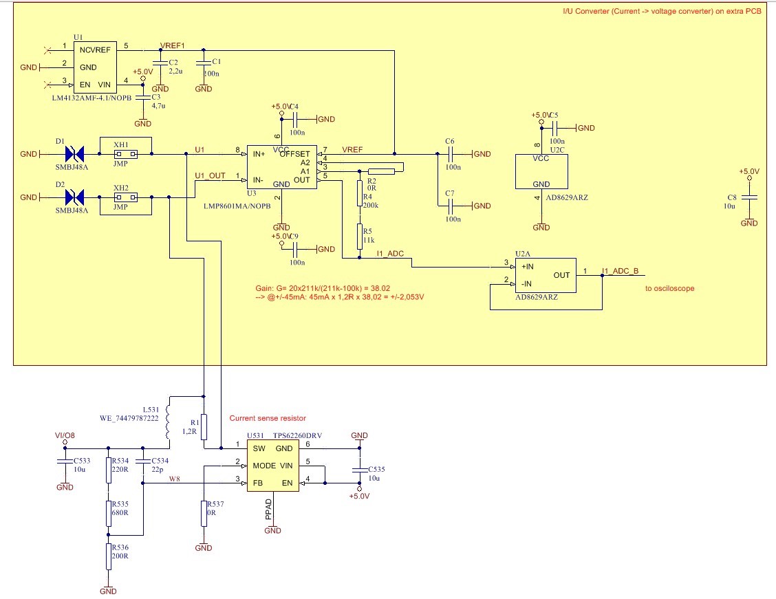
    Enclosed are more pictures. The current is not the correct load current, but the current through the inductance. A 1.2 Ohm resistor between SW pin and inductance was set and the current was measured by means of an I / U converter. It is currently not possible to measure the real load current.
    The pictures look slightly different than the originals, because I always have to make slight changes (solder wires, etc.).
    Finally, I just exchanged the two ICs again today, and so did the error again. Thus, I exclude the rest of the circuit again as a source of error (short circuit or low impedance load).

    Best regards

    Jens

  • Hello,
    I had a look, and the behavior of the current that you measured is unexpected for me. Can you clarify what you meant precisely: "The current is not the correct load current, but the current through the inductance. A 1.2 Ohm resistor between SW pin and inductance was set, and the current was measured by means of an I / U converter."
    Can you explain to me better which technique did you used to measure the inductor current? Maybe a schematic could be useful.
    Any chance to lift the inductor, add a wire, and use a current probe?


  • Hello,

    I lifted up the inductance and put a current sense resistor between the SW pin und the inductance. From the resistor two wires goes to a pcb board, where a TI current to voltage converter is mounted. From there it goes to the voltage probe of an oscilloscope.

    Attached are two circuit diagrams. The sense resistance has no influence on the behaviour of the DC / DC converter

    To lift up the part is not the problem (I have it already done), but I have no current probe. But I willask via a mail in our company.

    Best reagrds

    Jens Gießler

    Normal application:

    Here is the circuit to measure the current.

  • Hello,

    do you have a part number and a manufacturer for such a current probe?

    Best regards

    Jens Gießler

  • The protection diodes D1 and D2 are not assembled.

  • Hello,
    I order to try to understand which is the root cause of this high ripple on the converter; it would be better if you can measure it with a current probe. Unfortunately, I can't recommend one in particular, but you can find on the catalog of the producer of your oscilloscope. That's to remove any doubt about some influence that your previous setup could have introduced. Further, I need the BoM based on the schematic of TPS62260 (sent before).
    The last test that you can try is the swap of the IC (with high ripple) on another good board (with no issue) and another swap of a (good) IC on the board that gives high ripple.

  • Hello,

    I have now got a current probe for an oscilloscope (on loan). That's why it took a while for the answer. Enclosed the pictures again. The pictures look slightly different. But the clock burst and the higher ripple in the "broken" converter persist. The "whole" converter is always only a single pulse. Cause could be, because at the last measurement after completion of the measurements, I had already exchanged the "defective" and the "whole" converter. Since it was made to see again, if then the error with changes. That was the case. I have already exchanged the DCD / DC twice. In both cases, the "error" went along.
    The BOM (according to our mounter) is as follows:

    C533, C535: 10uF 0805: GCJ21BR71A106KE01L Murata: www.mouser.com/.../c03e-516224.pdf
    -------------------------------------------------- -------------------------------------------------- -----
    C534: 22pF 0402: 885012005057 Würth: katalog.we-online.de/.../885012005057.pdf
    -------------------------------------------------- -------------------------------------------------- -----
    R535: 680R 0603: 0603SAF6800T5E Royal electronic
    -------------------------------------------------- -------------------------------------------------- -----
    R536: 200R 0603: 0603SAF2000T5E Royal electronic
    -------------------------------------------------- -------------------------------------------------- -----
    R534: 220R 0603: 0603SAF2200T5E Royal electronic
    -------------------------------------------------- -------------------------------------------------- -----
    R537: 0R 0603: RC0603FR-070RL Yageo
    -------------------------------------------------- -------------------------------------------------- -----
    L531: 74479787222 Würth: katalog.we-online.de/.../74479787222A.pdf
    -------------------------------------------------- -------------------------------------------------- -----


    Load:
    2 x 100nF 0402: CL05B104K05NNND Samsung
    1 x 4.7uF 0603: CL1DA475KP8NNNC Samsung
    1 x CION-LX (Goepel electronic, ASIC)

    Best regards
    Jens

    3_Measurement.zip

  • Hello,

    I have now got a current probe for an oscilloscope (on loan). That's why it took a while for the answer. Enclosed the pictures again. The pictures look slightly different. But the clock burst and the higher ripple in the "broken" converter persist. The "whole" converter is always only a single pulse. Cause could be, because at the last measurement after completion of the measurements, I had already exchanged the "defective" and the "whole" converter. Since it was made to see again, if then the error with changes. That was the case. I have already exchanged the DCD / DC twice. In both cases, the "error" went along.
    The BOM (according to our mounter) is as follows:

    C533, C535: 10uF 0805: GCJ21BR71A106KE01L Murata: www.mouser.com/.../c03e-516224.pdf
    -------------------------------------------------- -------------------------------------------------- -----
    C534: 22pF 0402: 885012005057 Würth: katalog.we-online.de/.../885012005057.pdf
    -------------------------------------------------- -------------------------------------------------- -----
    R535: 680R 0603: 0603SAF6800T5E Royal electronic
    -------------------------------------------------- -------------------------------------------------- -----
    R536: 200R 0603: 0603SAF2000T5E Royal electronic
    -------------------------------------------------- -------------------------------------------------- -----
    R534: 220R 0603: 0603SAF2200T5E Royal electronic
    -------------------------------------------------- -------------------------------------------------- -----
    R537: 0R 0603: RC0603FR-070RL Yageo
    -------------------------------------------------- -------------------------------------------------- -----
    L531: 74479787222 Würth: katalog.we-online.de/.../74479787222A.pdf
    -------------------------------------------------- -------------------------------------------------- -----


    Load:
    2 x 100nF 0402: CL05B104K05NNND Samsung
    1 x 4.7uF 0603: CL1DA475KP8NNNC Samsung
    1 x CION-LX (Goepel electronic, ASIC)

    Best regards
    Jens

    8802.3_Measurement.zip

  • Hello,

    To support you further I invite you to contact me by email: a-furio@ti.com

  • Hello,

    since we started a communication via mail, I am going to close this post.